Why USB Type-C Circuit Protection is Vital and How to Implement It
Contributed By DigiKey's North American Editors
2017-08-08
Universal Serial Bus (USB) Type-C™ has introduced a compact, reversible data and power connector that also supports USB Power Delivery (USB PD). Supporting up to 100 watts (20 volts @ 5 amps), USB PD is helping to drive a rapid gain in popularity for USB Type-C as it can, among other features, quickly charge Li-ion batteries.
However, as with all versions of USB technology, electrostatic discharge (ESD) poses a risk to a USB Type-C system’s sensitive silicon. USB Type-C also introduces some unique safety challenges: high power delivery, compact connectors, and the ease with which consumers can attach non-compliant cables has markedly increased the number of overvoltage failure mechanisms for the technology, to the point where reliable circuit protection is vital.
This article outlines the need for USB Type-C circuit protection and introduces some sample protection circuits and components. It then explains how to design and implement protection circuitry that safeguards such systems against all ESD and overvoltage failure modes.
For more details on USB PD itself, refer to the library article, “Designing in USB Type-C and Using Power Delivery for Rapid Charging”.
What can go wrong with USB Type-C?
Implementing ESD protection for all USB systems is good design practice. Several standards govern ESD discharge robustness in USB systems (and elsewhere). For example, EN 55024 (“information technology equipment - immunity characteristics - limits and methods of measurement”) requires resilience to 4 kV on contact, and 8 kV across an air gap (criteria B: temporary perturbation and self-recovery).
In addition to the ESD risks which afflict all USB systems, USB Type-C introduces some unique failure modes. These modes are due to a combination of two factors: USB PD high power delivery and compact geometry.
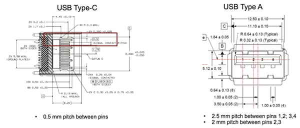
The high-power delivery enabled by USB PD can be adopted by legacy USB systems provided they employ the USB 2.0 or 3.0 communication protocol. However, the failure risk in non-USB Type-C applications is mitigated to an extent by the more relaxed geometry of legacy USB connectors (Figure 1).
Figure 1: USB Type-C’s popularity is partly based on its compact, reversible connector. The downside is a reduced pin pitch compared with older USB connector, such as USB Type-A. The reduced pin pitch of Type-C increases the probability of shorts. (Source: www.USB.org)
A USB Type-C connector features a pitch between pins of just one quarter that of a Type A connector. The reduced pin pitch heightens the chance that twisting the cable or removing the connector while it’s subject to a high current/voltage can cause catastrophic shorts. A build-up of debris inside the connector can have a similar catastrophic effect.
In addition, the popularity of the Type-C has spawned a wide range of third-party cables and power adapters. Many of these are not capable of handling the high currents supported by USB Type-C and USB PD standards.
Mechanical stress on a compact connector, debris, and non-compliant cables coupled with high current/voltage increases the risk of a short circuit in USB Type-C systems compared to other versions of USB technology. If such a short circuit occurs between the connector’s adjacent VBUS and CC or SBU pins, downstream circuitry can be subject to a damage inducing 20 volt surge (Figure 2).
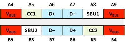
Figure 2: This section through a USB receptacle (all pins not shown) illustrates the proximity of CC (Connection/Configuration) pins and SBU (sideband/audio adapter accessory configuration/additional function to be defined) pins are to the bus power supply (VBUS). (Image source: STMicroelectronics)
The risk of short circuits, to PD controllers in particular, is high because the devices are connected directly to the CC pins and are designed to operate to a maximum of 5 volts. Protection for these devices is important because PD controllers are used to negotiate maximum current and voltage levels between charger and unit under charge during USB PD operation. Incorrect operation of USB PD due to PD controller damage could be a safety hazard. For example, an unprotected wall adapter with a short circuit would expose a downstream PD controller to damage (Figure 3).

Figure 3: A faulty wall adapter can short between VBUS and CC pins exposing a downstream PD controller to a damaging 20 volts. (Diagram drawn using DigiKey Scheme-it®, based on original source image from Texas instruments)
ESD circuit protection
USB Type-C ESD protection can be implemented relatively easily by using transient voltage suppression (TVS) diodes fitted between all the USB Type-C plug and receptacle pins and ground. Careful choice of a TVS diode is required because the devices need to be high-voltage DC tolerant to cope with all USB PD charging events.
STMicroelectronics’ ESDARF02-1BU2CK bidirectional single-line TVS diodes are a good match for this application. During a +8 kilovolt (kV) ESD event, the devices clamp the line to 19 volts within 30 ns and 15 volts in 100 ns (Figure 4). Yet the diodes can tolerate the 20 volts DC that routinely occurs during USB PD operation.
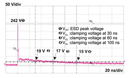
Figure 4: STMicroelectronics’ ESDARF02-1BU2CK TVS diode response to +8 kV ESD surge. Peak voltage is limited to 242 volts and the voltage drops to 19 volts in 30 ns. The diode can also tolerate high-voltage DC during USB PD operation. (Source: STMicroelectronics.)
STMicroelectronics offers an evaluation kit, the STEVAL-OET004V1, which allows the designer to experiment with ESD protection solutions that range from using TVS diodes alone, to one using a combination of ECMF04 and ECMF02 common-mode choke filters and TVS diodes to preserve signal integrity when the USB Type-C connection is used for very high speed data transfer.
While high-voltage DC tolerant TVS diodes and common-mode filters offer good protection against transient ESD events, the clamping voltage is typically much higher than the 5 volt limit specified for components such as USB PD controllers. That makes TVS diodes alone unsuitable for protection against sustained high voltages such as those that occur with short circuits.
Overvoltage circuit protection
For comprehensive USB Type-C circuit protection, ESD protection must be supplemented with overvoltage protection (OVP) to safeguard against short circuits. On first inspection, such OVP would seem to only have to deal with peak voltages of 20 volts since that is the most that could occur in a VBUS-based short circuit.
However, this isn’t always the case. For example, the inductance of a one meter USB cable is sufficient to generate ringing that can result in a peak voltage of double the steady state short circuit voltage. In a USB Type-C system using USB PD at 20 volts, up to 40 volts could be conducted on the CC or SBU lines during a VBUS-to-short event. USB Type-C OVP must cater to these higher than expected peak voltages.
One relatively straightforward option for USB Type-C OVP is to employ N-channel MOSFETs (nMOSFETs), paired with an OVP device.
The OVP device drives the nMOSFET gate high when the monitored input is below the user adjustable overvoltage threshold allowing current to flow. When the input voltage exceeds the overvoltage threshold, which would occur during a short circuit, the nMOSFET is pulled low, disconnecting the load from the input. In addition to the OVP device, the protection solution requires a charge pump to maintain the 6.5 to 8 volt gate voltage. This voltage is needed to let the nMOSFET operate in the low resistance region to accommodate the 5 volt DC of normal USB Type-C operation.
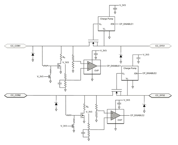
The situation is further complicated when a VBUS-to-short event occurs that bypasses the cable. Because the inductance of the receptacle in this “no-cable” scenario is so low, the rise time to reach 90% of the peak voltage of the short circuit can be less than 10 nanoseconds. Such a sudden rise is beyond an nMOSFET’s reaction time, exposing downstream components to damaging voltages. The cable bypass also lowers the receptacle’s resistance, exposing the system to a much higher current compared with that when a cable is present. Additional clamping components are therefore required to protect against these types of short circuits (Figure 5).
Figure 5: ESD and OVP circuit schematic for USB Type-C CC1 and CC2 pins. The solution for each line includes an nMOSFET, OVP device, charge pump, and clamping components. Similar protection would be required for SBU lines. (Image source: Texas Instruments)
Based on an nMOSFET, OVP device, charge pump, and clamping components, the protection circuit comprises approximately 15 discrete parts for each CC pin. Similar circuits would also be required to protect SBU lines. This translates to a large bill of materials (BOM), just for protection.
Simplifying protection (and shortening the BOM)
USB Type-C circuit protection can be simplified by replacing discrete component solutions with a monolithic device such as Texas Instruments’ TPD8S300. The device integrates an entire VBUS-to-short OVP and ESD protection system in a 3 by 3 mm QFN package solution (Figure 6).
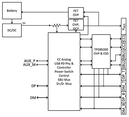
Figure 6: This application circuit shows how a single TPD8S300 can provide ESD and OVP safeguards for a downstream USB PD controller. (VBUS requires additional ESD and OVP protection for a comprehensive solution.) (Image source: Texas Instruments)
Instead of a complex discrete solution, an engineer can add just one TPD8S300 to a USB Type-C implementation to meet their entire IEC 61000-4-2 ESD and VBUS-to-short OVP requirements. The TPD8S300 includes four channels of VBUS-to-short protection (for CC and SBU pins), eight channels of ESD protection (for the CC, SBU, and USB 2.0 pins), and dead battery resistors. The response of the circuit of Figure 6 is such that the Voltage on the CC1 pin peaks at 6.5 volts, but is clamped to 0.5 volts in less than 100 nanoseconds (Figure 7).
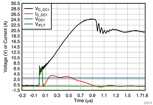
Figure 7: Response of the application circuit in Figure 6 to a 20 V short circuit between VBUS and CC1. Voltage on the CC1 pin (green line) peaks at 6.5 V but is clamped to 0.5 V in less than 100 ns. (Image source: Texas Instruments)
Conclusion
USB Type-C systems with USB PD carry up to 20 volts and 5 amps. Combined with compact connectors and receptacles featuring narrow pin pitches, such high voltage and current amplify the risk of shorts (particularly on the CC and SBU pins that sit adjacent to the VBUS rail), making OVP protection mandatory.
Comprehensive ESD and OVP for USB Type-C systems can be achieved using discrete components, but such an approach results in solutions with dozens of components that can be hard to accommodate both within the BOM and the space allocated to the solution.
As shown, an alternative approach, which integrates ESD and OVP circuits into a single chip, considerably eases design and reduces solution size.
References
- “USB Type-C protection and filtering”, Application note AN4871, STMicroelectronics, December 2016.
- “Circuit Protection for USB Type-C”, Padmanabhan Gopalakrishnan, Michael Koltun IV, Texas Instruments, October 2016.

Disclaimer: The opinions, beliefs, and viewpoints expressed by the various authors and/or forum participants on this website do not necessarily reflect the opinions, beliefs, and viewpoints of DigiKey or official policies of DigiKey.


