Use Programmable Power Modules to Accelerate DC/DC Regulator Design
Contributed By DigiKey's North American Editors
2020-08-19
Switching DC-DC voltage regulators bring high efficiency to power supplies. While there’s a wide variety of good-quality monolithic regulators available, each is designed to meet the needs of a range of applications rather than the unique specifications of an engineer’s own design. Alternatively, optimizing the power supply for a particular application demands time-consuming and expensive design iterations.
What designers need is a web-based interface to a power supply vendor that allows them to configure their power supply design with the performance parameters they require—and then have it shipped in bulk once the design is frozen.
This article describes one such design process when using configurable power modules. Specifically, the article will describe how MPS' evaluation kit (EK) and web-based software can be used to accelerate the design process for a simple or more advanced DC-DC converter design.
Getting started with DC-DC converter design
It is entirely possible to design a step-down (buck) switching voltage regulator from scratch and with relatively few components. For example, a basic design comprises one transistor—which is essentially used as a switch—one diode, one inductor, a capacitor across the output, and another one across the input. However, for a practical solution, several additional elements will likely be needed, including a voltage reference, error amplifier, comparator, oscillator and switch driver. But few engineers choose to go down the path of designing from discrete components because there is such a wide range of proven and inexpensive highly-integrated monolithic DC-DC voltage regulators available.
It is often easier to select a regulator from an established supplier based on the requirements of the specification such as input and output voltage, maximum load current, and maximum voltage ripple, with factors such as efficiency, transient response and frequency response coming into play for advanced designs. While chip makers do offer an impressive range of solutions satisfying most parts of the specification, it’s impossible for them to supply a device perfectly matched to every eventuality. That leaves the designer with some work to do.
The amount of work depends on the degree of integration of the monolithic solution, but a typical starting point for a low-current (under 10 amperes (A)) design is a chip that integrates the pulse width modulation (PWM) controller, switching elements (MOSFET power transistors) and bypass diode(s), leaving the designer to specify the external inductor, bypass capacitors and other passive components required for input and output filter circuits.
Although there’s a lot of information on how to go about designing a power supply based around a monolithic regulator from manufacturers and other sources (including the recommended reading list below), it’s still a tricky and tedious process involving calculation and then several cycles of hardware prototyping to see how the theoretical circuit performs in practice, and then adjusting it to precisely meet the specification.
MPS offers an alternative route to this time-consuming power supply design process with its configurable power modules.
Introduction to configurable power modules
At the heart of the MPS mEZDPD3603A configurable power module is a high-frequency, synchronous, rectified, buck converter with an I2C control interface, a multipage one-time programmable (OTP) ROM memory, and 3 A continuous output current capability. The converter integrates high-side and low-side power MOSFETs, compensation networks and a feedback divider. Output voltage level, voltage slew rate, switching frequency, enable, and power saving modes are programmable via an I2C interface, enabling the designer to optimize each output for their particular design.
Current-mode operation provides fast transient response and eases loop stabilization. Full protection features include under-voltage lockout (UVLO), over-voltage protection (OVP), over-current protection (OCP), and over-temperature protection (OTP).
The mEZDPD3603A module adds almost all the peripheral components needed for a working design to this buck converter (Figure 1).
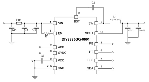 Figure 1: Internal schematic of the MPS mEZDPD3603A module. All that’s left for the designer to do is specify the values of the input (CIN) and output (COUT) capacitors. (Image source: MPS)
To complete a fully-functioning DC-DC buck regulator power supply design, all the designer needs to add are the input (CIN) and output (COUT) capacitors. When designing from scratch, calculating the value of these capacitors is not simple and is influenced by output voltage, load, duty cycle, and voltage ripple (see DigiKey technical article. “Capacitor Selection is Key to Good Voltage Regulator Design”). But in the case of the MPS module, the manufacturer has calculated the values for the designer. Final selection is only influenced by output voltage (Figure 2 and Table 1).
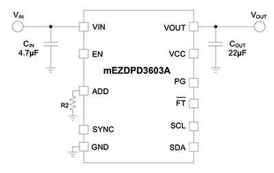 Figure 2: In an MPS mEZDPD3603A typical application circuit, R2 is used to set the I2C address to allow identification of multiple modules in a system. (Image source: MPS)
|
Table 1: Recommended capacitor values are shown for the application circuit of Figure 2 for various output voltages. (Image source: MPS)
If the power supply is to be employed in a product covered by strict electromagnetic interference (EMI) regulations, the input capacitor can be replaced with an L-C filter circuit comprising three capacitors and an inductor. (For more about input and output filter circuit design see DigiKey technical article “Use Low-EMI Switching Regulators to Optimize High-Efficiency Power Designs”.) The value of these components again depends on the output voltage, and once more the manufacturer has provided the answers. (Figure 3 and Table 2.)
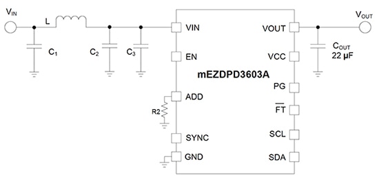 Figure 3: MPS mEZDPD3603A application circuit with EMI filtering for EN55022 Class B standard. (Image source: MPS)
|
Table 2: Recommended component values for application circuit above for various output voltages. (Image source: MPS)
The module offers an input voltage range of 4.5 to 36 volts with an output of 0.6 to 12 volts. Voltage accuracy is ±1% and line and load regulation (VIN = 24 volts, VOUT = 5 volts) is ±1%. Maximum current is up to 3 A and output voltage ripple (VIN = 24 volts, VOUT = 5 volts, full load) is 30 millivolts (mV). Table 3 summarizes the module’s performance and efficiency figures, while VOUT for various efficiency and load current values is shown in Figure 4.
|
Table 3: MPS mEZDPD3603A performance parameters. (Image source: MPS)
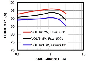 Figure 4: MPS mEZDPD3603A efficiency figures for VIN = 24 volts and VOUT = 3.3, 5, and 12 volts. (Image source: MPS)
Configurable power module evaluation kit
Because the MPS module includes digital logic circuitry, its operational performance can be modified by changing software parameters. Access to the parameters is via the module’s I2C interface, from where settings in the device’s RAM can be interrogated and changed. Once the desired optimal setting has been reached, the OTP ROM memory allows the settings to be permanently stored.
MPS provides hardware and software tools to support design with the configurable power modules. The primary tool is the PKT-MEZDPD3603A hardware EK. The EK measures 64 by 64 millimeters (mm) and includes input and output capacitors (and an optional EMI filter if required), plus a connector into which the configurable power module is plugged. Once the module is connected, an appropriate load and a power supply providing the desired input voltage (between 4.5 and 36 volts) needs to be connected to the EK (Figure 5).
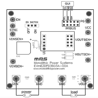 Figure 5: The configurable power module evaluation kit includes a socket for the module and requires an external power supply and load. (Image source: MPS)
The EK also requires a connection to a PC to allow for configuration from MPS’s Virtual Bench V3.0 software. The company provides a USB (PC end) to I2C (EK end) dongle for this purpose. A USB cable connects the dongle to the PC and a 10-pin ribbon cable does the job on the other side. The EK’s I2C interface connects directly to the module’s I2C pins and enables configuration from the PC (Figure 6).
 Figure 6: The configurable power module EK requires a power supply, load and connection to a PC via a USB to I2C dongle. (Image source: MPS)
Programming the power module
Once the hardware is connected to the PC (running Windows XP, 7 or later) and Virtual Bench V3.0 is installed on the computer and started up, the developer is presented with two options: “Simulation & Program” (which allows the developer’s configuration to run on a software simulator rather than the EK hardware) and “Direct Programming Mode.” The following discussion focuses on the direct programming option because it allows the developer to directly configure the module at the heart of the EK hardware.
There are two types of configurations available from Virtual Bench V3.0: Basic and Advanced. Under the Basic configuration, the developer can read the existing settings for output voltage (volts), inductor value (in microhenries (µH)), switching frequency (in kilohertz (kHz)), and the operating mode (for example, peak current-mode). The developer can then make changes to these settings, program the module’s RAM with the revised numbers, and power up the module to check the impact of changes on its performance.
Similarly, under the Advanced tab, the designer is able to interrogate and change the settings for more detailed performance parameters, under the following groupings:
- Light-Load mode: The available modes are Advanced Asynchronous Modulation (AAM) and Forced Continuous Current Mode (CCM). AAM optimizes converter efficiency during light-load or no-load conditions, while forced CCM keeps the switching frequency constant with a smaller output ripple (but is less efficient than AAM under light loads).
- Compensation: These settings alter the regulator’s frequency response which determines the device’s transient response, precision, and stability, and in turn how well it maintains a set voltage output under variations in the input voltage, load, and duty cycle. Good compensation leads to a power supply that’s stable over a wide frequency range yet is not overcompensated so that its dynamic response is poor.
- Switching: These settings alter the rising and falling voltage slew rates as the regulator switches, and frequency dithering time and amplitude. Slew rate and dithering are both important for minimizing EMI.
- VIN/EN threshold: These settings determine the threshold limits (and hysteresis) of the input voltage UVLO and EN operation.
- Power good: These settings determine the upper and lower rising thresholds and hysteresis of “Power Good.”
- SS Time: Setting for soft start. Soft start prevents the regulator from overloading the input when the output is turned on.
- Protection: These settings allow the designer to implement protection modes and thresholds such as peak current, OVP and OTP (Figure 7).
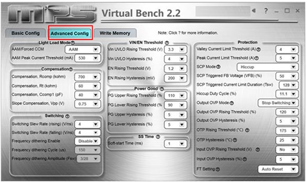 Figure 7: MPS’s Virtual Bench GUI includes advanced programming of the configurable module to optimize its performance to meet the designer’s specification. (Image source: MPS)
Once the designer has selected the best settings for the application, the information is written to the module’s built-in RAM. The developer can then run the EK under various loads to check its performance. It’s a simple matter to modify the settings and rewrite to RAM in order to optimize the power supply’s performance.
Because RAM is volatile, once the module is switched off, the settings are lost. Upon restarting, the module starts up with factory default settings. It is possible to export the information in RAM to Virtual Bench prior to power down for future reference.
Once the optimum settings are determined, the designer can then program these into the OTP ROM such that they are retained on power down and used the next time the module starts up. The EK still allows further experimentation of settings via the I2C interface and RAM, but after the first use of the ROM, no further settings can be saved.
Conclusion
While a wide range of excellent monolithic voltage regulators is available, the designer still faces a lot of work to design and test the peripheral circuits that optimize the performance of the design for a particular application. By combining a complete hardware design in a module with programmable digital logic, MPS’s configurable programmable modules ease and accelerate this design loop.
As shown, an EK combined with a PC-based GUI makes the configuration simple, and the designer can either make basic settings such as output voltage or current and leave the rest at factory default or engage in more advanced switching converter design to minimize EMI and transient response while maximizing stability and efficiency.
Once the design is frozen, production quantities of the module can be supplied non-programmed for the customer to configure from the prototype data, or, if the configuration information is supplied to MPS, the modules can be programmed at the factory and supplied ready-to-go.
Recommended reading
- Capacitor Selection is Key to Good Voltage Regulator Design.
- Use Low-EMI Switching Regulators to Optimize High-Efficiency Power Designs.
- Understanding Switching Regulator Control Loop Response.
- Designing Compensator Networks to Improve Switching Regulator Frequency Response.
- The Difference Between Switching Regulator Continuous and Discontinuous Modes and Why It's Important.

Disclaimer: The opinions, beliefs, and viewpoints expressed by the various authors and/or forum participants on this website do not necessarily reflect the opinions, beliefs, and viewpoints of DigiKey or official policies of DigiKey.


