Use Coupled Inductors in Multiphase Buck Converters to Improve Efficiency
Contributed By DigiKey's North American Editors
2025-04-23
Multiphase buck converters are widely used in 12 V applications such as datacenters, artificial intelligence (AI) systems, and communications infrastructure. A common theme across these use cases is the need for improved efficiency without compromising performance or increasing the physical footprint.
One promising approach involves coupled inductors (CLs). By using mutual inductance between phases, CLs enable superior current ripple cancellation, resulting in significant efficiency improvements while preserving compatibility with conventional layouts.
This article briefly outlines the efficiency and layout challenges facing designers of multiphase buck converters. It then introduces CLs, presents experimental results validating the efficiency improvements, and shows how they are applied in converters from Analog Devices.
Conventional multiphase buck converter efficiency challenge
In high-performance computing and communications systems, efficiency losses in power delivery can have outsized impacts on system cost, reliability, and thermal management. Designers of conventional multiphase buck designs often face challenges in this regard, particularly under light-load conditions where switching and AC losses become more pronounced.
At the same time, power-stage layout and mechanical constraints limit the options available for improving performance. In many systems, there is little room to increase component size, and changes to the printed circuit board (pc board) layout may not be feasible in the face of common footprint strategies.
As a result, there is strong interest in approaches that can deliver higher efficiency without requiring substantial changes to the power architecture. Ideally, such solutions would retain the same footprint, allow the use of existing output capacitance (CO), and maintain transient performance across a wide range of load conditions.
CLs address these demands by enabling ripple reduction and switching loss improvements, all within the same physical footprint as conventional designs.
How CLs improve power conversion
CLs offer an effective way to improve efficiency in multiphase buck converters without altering the layout. Unlike conventional designs that treat each phase as electrically independent, CLs share a standard magnetic structure that enables interaction between phases.
Two key parameters govern this interaction: leakage inductance (Lk) and mutual inductance (Lm). The leakage inductance behaves like the phase inductance (L) in traditional designs, while the mutual inductance introduces magnetic coupling across phases. As current increases in one phase, it induces a voltage in the others that opposes their current change, resulting in significant ripple current cancellation.
Equations 1 and 2 define the expected ripple current for conventional discrete inductor (DL) designs (dILDL) and CL designs (dILCL). These currents depend on the input and output voltages (VIN, VO), inductances L, Lk, and Lm, switching frequency (FS), and a “figure of merit” (FOM).
 Equation 1
") Equation 2
Equation 2
Where:
ρ = the coupling coefficient = Lm/L
D = duty cycle
Nph = the number of coupled phases
Equation 3 lays out the calculations for the FOM. This equation captures the extent of ripple cancellation as a function of various parameters. Specifically, the FOM depends on ρ, Nph, and D.
 / 1- [(Nph - 2 x j - 2) + j x (j+1)/ Nph x D + Nph x D x (Nph -2 x j-1) + j x (j +1)/Nph x (1 - D)] x ρρ+1/Nph-1") Equation 3
Equation 3
Where:
j = floor (D × Nph)
While the FOM depends on many factors, the coupling coefficient ρ plays a significant role. To illustrate this point, it is helpful to consider a practical example.
Evaluating ripple current for coupled inductors
Figure 1 illustrates FOM values for an application with a VIN of 12 V and a VO of 1 V, with a D of ~0.083 and conventional DL values of 100 nanohenries (nH). To upgrade this design to a CL while maintaining the transient performance with the same CO tank, the Lk for the CL must be 100 nH. This leaves Lm as the design variable. Higher values of Lm lead to lower ripple, but a conservative Lm of 260 nH is sufficient to achieve most of the desired benefits.
 Figure 1: Shown are the FOM values for a 4-phase CL for various Lm/Lk values as a function of D; the region of interest is highlighted. (Image source: Analog Devices, Inc.)
Even with this fairly conservative design, the ripple reduction is sufficient to enable lower switching frequencies. This is illustrated in Figure 2, which compares the current ripple for different inductor configurations and switching frequencies. The graph demonstrates that a CL operating at 400 kilohertz (kHz) maintains lower ripple than a conventional design at 800 kHz.
 and CL = 4 × 100 nH (800 kHz, 400 kHz)") Figure 2: Current ripple for DL = 100 nH (800 kHz) and CL = 4 × 100 nH (800 kHz, 400 kHz) for VIN = 12 V as a function of VO. (Image source: Analog Devices, Inc.)
Figure 2: Current ripple for DL = 100 nH (800 kHz) and CL = 4 × 100 nH (800 kHz, 400 kHz) for VIN = 12 V as a function of VO. (Image source: Analog Devices, Inc.)
The reduced switching frequency directly translates to lower switching losses, which include transistor switching losses, dead-time losses in MOSFET body diodes, reverse recovery losses, and gate drive losses. These frequency-dependent losses decrease proportionally as the switching frequency is reduced, resulting in substantial efficiency improvements.
Efficiency gains are most visible at light loads, where AC losses are more prominent due to their fixed nature regardless of output current. However, the benefits extend across the entire load range. Figure 3 shows experimental results comparing an 8-phase system with coupled inductors at 400 kHz against a conventional design at 600 kHz, demonstrating approximately 1% improvement at peak efficiency and 0.5% improvement at full load.
 and 2 × CL = 4 × 100 nH (solid curves)") Figure 3: Shown is a measured efficiency comparison of the 8-phase DL = 100 nH (dashed curves) and 2 × CL = 4 × 100 nH (solid curves) designs with a common footprint. (Image source: Analog Devices, Inc.)
Figure 3: Shown is a measured efficiency comparison of the 8-phase DL = 100 nH (dashed curves) and 2 × CL = 4 × 100 nH (solid curves) designs with a common footprint. (Image source: Analog Devices, Inc.)
Improving efficiency without sacrificing transient response
Notably, these efficiency improvements are achieved without compromising transient performance. Figure 4 illustrates the transient behavior of a 4-phase buck converter, comparing waveforms from an 8-phase design with discrete inductors (DL = 100 nH at 600 kHz) and a configuration using two CLs, each serving 4 phases (2 × CL = 4 × 100 nH at 400 kHz) with VIN = 12 V, VO = 0.9 V for 135 A load steps. Using the same current slew rate and CO results in comparable transient responses.
 and 2 × CL = 4 × 100 nH (400 kHz) (click to enlarge)") Figure 4: Shown is the transient for 8-phase DL = 100 nH (600 kHz) and 2 × CL = 4 × 100 nH (400 kHz) for VIN = 12 V, VO = 0.9 V for 135 A load steps; same board, same CO, same conditions. (Image source: Analog Devices, Inc.)
Figure 4: Shown is the transient for 8-phase DL = 100 nH (600 kHz) and 2 × CL = 4 × 100 nH (400 kHz) for VIN = 12 V, VO = 0.9 V for 135 A load steps; same board, same CO, same conditions. (Image source: Analog Devices, Inc.)
While the lower switching frequency of the CL might typically reduce feedback bandwidth, two factors counteract this limitation: the inherent advantages of the multiphase architecture and the enhanced phase margin provided by the coupled design. This phase margin improvement occurs because all coupled phase currents respond simultaneously when the duty cycle changes in response to a transient event in one phase.
Lower losses lead to better thermal performance, which can, in turn, enhance long-term reliability and potentially reduce cooling requirements in thermally constrained systems. All these benefits are achieved while maintaining compatibility with existing layouts.
Selecting components for multiphase buck converters
To implement an efficient multiphase buck converter, attention can be focused on three key components: the voltage regulator controller, the power stage integrated circuit (IC), and the CL. The controller manages phase timing and synchronization, the power stage handles high-current switching, and the CL enables ripple cancellation, driving improved efficiency.
For the controller, the Analog Devices’ MAX16602GGN+T (Figure 5) is a solid pick. Offered in a 56-QFN (7 mm × 7 mm) package, this device supports an 8-phase rail and a separate single-phase rail. Notable features include autonomous phase shedding, telemetry via PMBus, integrated fault protection and logging, and an internal 1.8 V bias regulator. These features enable precise control, reduced component count, and enhanced transient response in multiphase voltage regulator systems.
 Figure 5: The MAX16602GGN+T voltage regulator controller supports up to 8 phases. (Image source: Analog Devices, Inc.)
The power stage can be implemented using Analog Devices’ MAX20790GFC+T (Figure 6). This smart power stage integrates MOSFETs, gate drivers, and current sensing into a single 12-FC2QFN (3.25 × 7.4 mm) package device. Operating at a switching frequency range of 300 kHz to 1.3 megahertz (MHz), it enables designers to optimize the performance of CL designs. Key features include telemetry and fault reporting through the controller PMBus, as well as advanced self-protection features.
 Figure 6: The MAX20790GFC+T smart power stage integrates MOSFETs, gate drivers, and current sensing into a single device. (Image source: Analog Devices, Inc.)
An example of a suitable CL is the Eaton CLB1108-4-50TR-R (Figure 7), which integrates four tightly coupled 50 nH phases into a single package. The component’s construction supports high saturation current and thermal performance, making it well-suited to demanding AI and data center workloads.
 Figure 7: The CLB1108-4-50TR-R is a 4 x 50 nH coupled inductor. (Image source: Eaton)
In a typical configuration, the MAX16602 controller would drive up to eight MAX20790 power stages, with each output phase connected to the corresponding winding of a dual 4-phase CL. Compared to conventional designs, this architecture delivers measurable improvements in power efficiency while maintaining the same physical footprint and transient performance.
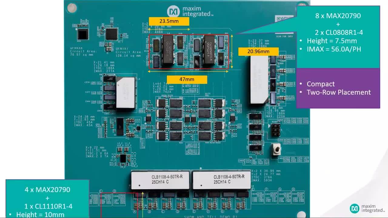
Testing coupled inductor designs with evaluation hardware
For designers looking to explore CL solutions, Analog Devices’ MAX16602CL8EVKIT# evaluation kit (Figure 8) provides a convenient platform for testing and development. This board is specifically designed to demonstrate the capabilities of the MAX16602 controller and MAX20790 power stage ICs in conjunction with coupled inductors.
 Figure 8: The MAX16602CL8EVKIT# can be used to explore multiphase buck converter designs. (Image source: Analog Devices, Inc.)
The evaluation kit is a practical reference design demonstrating how these components can be integrated effectively. It includes all the necessary circuitry to support an 8-phase power conversion solution and incorporates comprehensive measurement points that enable monitoring of key parameters such as transient response.
Conclusion
CLs offer significant advantages for multiphase buck converter designs. By introducing mutual inductance between phases, these components enable substantial ripple current cancellation, allowing for reduced switching frequency and improved overall efficiency. Importantly, these gains can be achieved without increasing the physical footprint or compromising transient performance. Combined with controller and power-stage chipsets, these solutions provide a practical path for designers transitioning from conventional topologies to more efficient, magnetically coupled alternatives.
Disclaimer: The opinions, beliefs, and viewpoints expressed by the various authors and/or forum participants on this website do not necessarily reflect the opinions, beliefs, and viewpoints of DigiKey or official policies of DigiKey.