Use an Automotive-Grade Flyback Transformer for Compact EV Power Supply Designs
Contributed By DigiKey's North American Editors
2025-06-12
The electrical and electronic power needs of innovative automotive designs can be summarized as follows: increased power, improved efficiency, reduced space requirements, and enhanced reliability. In the case of electric vehicles (EVs), efficiency is crucial in helping to alleviate “range anxiety” for users. The combination of requirements in the context of EVs translates to compact and lightweight power solutions for standby and auxiliary power sources. Smaller power supplies introduce additional challenges, including the need for greater isolation to prevent electrical breakdowns between closely spaced components and reduced electromagnetic interference (EMI).
Flyback power converters are commonly used in various low-power EV applications, including generating auxiliary power, battery management, and gate-drive power. They offer simpler designs with fewer components, which reduce size, increase reliability, and lower costs. The heart of any flyback power supply is the flyback transformer, which is generally among one of the largest components required to support high voltage isolation.
This article describes how flyback converters operate, the effects of inductive and capacitive parasitics, and the importance of component size and signal isolation. It then introduces a flyback transformer from Bourns and shows how it can help address numerous automotive power challenges.
The flyback converter
Flyback converters are noted for their simple, minimal component design, for power levels up to 100 W. At the heart of these designs is a flyback transformer, which provides both power transfer and isolation between the primary and secondary sides of the converter circuit (Figure 1, top). The converter can step up or down the voltage of a DC power source based on the flyback transformer configuration. In addition to the flyback transformer, the circuit requires a primary-side switch (SW), typically a MOSFET, and a secondary rectifier/filter.
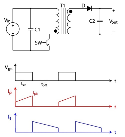 Figure 1: Shown is a simplified schematic of a flyback converter's basic elements (top) and the significant operational waveforms (bottom). (Image source: Bourns Inc.)
The operating cycle begins when SW is turned on by placing Vgs in a high state (Figure 1, bottom). The switch closes, and the voltage applied across the inductor is a step function. The inductor opposes any instantaneous change in the current and serves to integrate the applied step voltage. This results in a ramp function, and the current in the primary winding of the flyback transformer increases linearly due to the effect of primary inductance. The transformer secondary has no current flow because the rectifier diode (D) is reverse-biased, and an air gap in the flyback transformer’s magnetic core prevents saturation as the transformer’s magnetic field increases.
When the switch is turned off, achieved by returning Vgs to the low state, the energy stored in the transformer's magnetic field is transferred to the secondary through the now forward-biased diode, charging the output capacitor (C2). The secondary current falls linearly until the energy from the magnetic field is depleted or the switch is turned on again, beginning the next cycle.
A typical transformer, as found in a linear power supply, continuously transfers energy from the primary winding to the secondary winding. The flyback transformer's operation is more similar to that of a pair of coupled inductors in that it does not transfer energy continuously during the operating cycle. However, like a transformer, the output voltage can be adjusted by varying the turns ratio between the primary and secondary windings. The flyback transformer also provides galvanic isolation between the primary and secondary windings. Additionally, it supports multiple secondary windings, allowing numerous output voltages from the converter.
Parasitic effects in flyback converters
Typical of electronic circuits, flyback converters suffer unwanted effects due to parasitic inductances and capacitances (Figure 2).
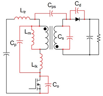 Figure 2: Shown is a schematic diagram of a flyback converter that highlights in red the parasitic capacitances and inductances associated with converter components. (Image source: Bourns Inc.)
The magnetizing inductance (Lm) is the main inductive property that determines the energy storage of the flyback transformer. Also associated with the transformer is a parasitic leakage inductance (Llk), which is in series with the switch. When the switch is opened, it tries to maintain the primary current and raises the voltage across the switch. Most flyback converters employ clamp circuits or snubbers to protect the switch from this transient voltage. This effect also increases magnetic field radiation and impacts EMI. Board trace inductance (Ltr) adds to these effects.
Transformer designers make every effort to minimize leakage inductance. The principal method is to increase the coupling between the primary and secondary windings. This is accomplished by minimizing the separation between the windings and also by interleaving them.
The distributed capacitances include the primary capacitance (Cp), interwinding capacitance (Cps), secondary capacitance (Cs), FET output capacitance (Co), and secondary diode capacitance (Cd). These capacitances interact with the inductances to reduce the integrity of the converter signal waveforms (Figure 3).
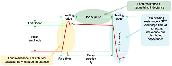 Figure 3: Shown are the effects of capacitive and inductive parasitic elements on the switching waveform. (Image source: Bourns Inc.)
The switching waveform ideally would be a rectangular pulse with no overshoot or undershoot. The fast transition times of this rectangular pulse guarantee that the voltage waveform is at zero before the current increases. In reality, the effects of parasitic capacitances and inductances slow the transition times and cause overshoot, undershoot, and ringing. In addition, slower rise and fall times increase the converter’s switching losses due to the overlap of the non-zero primary voltage and current waveforms. This overlap dissipates power as switching losses in the FET switch, thereby lowering the converter's efficiency. The noticeable droop in the pulse top is due to the load resistance and magnetizing inductance.
When designing a flyback transformer, significant effort must be made to keep the self-resonant frequencies away from the converter’s switching frequencies, and keeping the wiring between the switch and the flyback transformer as short as possible helps minimize parasitic capacitance. Additionally, the interwinding capacitance provides a path for coupling the high-frequency components of the primary signal to the output. The greater the interwinding capacitance, the greater the converter’s conducted EMI emissions. Optimal performance requires a design trade-off, as closer coupling of the windings decreases the leakage inductance but also increases the interwinding capacitance. This is where the experience of the transformer designer matters.
Size reduction and signal isolation
Components intended for automotive applications should be as small as possible. The physical size of a component is determined by the materials' characteristics and the physics of the part’s function. In the case of the flyback transformer, the spacing of conductors has to be sufficient to handle the peak working voltages and the voltage testing required for standards certification. The key specifications associated with voltage breakdown are clearance and creepage (Figure 4).
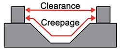 Figure 4: Clearance and creepage are specifications that describe the minimum distances between adjacent conductors needed to prevent electrical breakdown and arcing. (Image source: Bourns Inc.)
Clearance is the shortest distance between two conductive paths in the air, and creepage is the shortest distance between two conductive paths along the surface of an insulating material. These distances are crucial in preventing arcing and maintaining electrical isolation.
Flyback transformer meets EV requirements
The Bourns HVMA03F40C-ST10S (Figure 5) flyback transformer is automotive-qualified and designed to operate at switching frequencies from 100 kHz to 400 kHz, and is rated to handle up to 3 W.
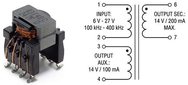 Figure 5: The HVMA03F40C-ST10S flyback transformer (left) is rated at 3 W and features dual output windings (right). (Image source: Bourns Inc.)
This flyback transformer is an automotive-grade, AEC-Q200-compliant component rated to operate over a temperature range of -40°C to +155°C (including self-temperature rise). It is an eight-pad surface-mount device with an exceptionally compact footprint of 9.5 mm × 10.3 mm, with a height of 13 mm. Designed to operate with a primary drive of 6 V to 27 V, its dual secondary windings produce a nominal output of 14 V.
The primary winding (between pins 1 and 2) offers a main inductance of 40 microhenries (mH) with a leakage inductance of only 1.1 mH and a series resistance of 1.0 ohms (Ω). The principal secondary (between pins 6 and 7) has a series DC resistance of 1.0 Ω. The auxiliary output (between pins 3 and 4) has a series resistance of 1.4 Ω. The transformer is set for unity gain with a turns ratio of 1:1:1.
Rated to handle a working voltage up to 900 V, its voltage isolation is 4,000 VAC. Despite the high voltage rating, the transformer has a rated creepage distance of 10 mm and a clearance distance of 6 mm.
This flyback transformer is suitable for automotive applications, such as transistor gate-drive power supplies, battery management circuits, or an isolated power source between independent power circuits in EVs. It is compatible with many flyback controller integrated circuits operating at a fixed switch frequency with pulse width modulation, or with fixed pulse width and variable frequency control.
Conclusion
The Bourns HVMA03F40C-ST10S is particularly well-suited to helping designers meet EV power requirements. It is AEC-Q200 compliant and features a compact form factor, compliance with clearance and creepage specifications, and a rating of 3 W over a wide temperature range.

Disclaimer: The opinions, beliefs, and viewpoints expressed by the various authors and/or forum participants on this website do not necessarily reflect the opinions, beliefs, and viewpoints of DigiKey or official policies of DigiKey.


