Understanding the Advantages and Disadvantages of Linear Regulators
Contributed By DigiKey's North American Editors
2017-09-20
Designers are well aware of the efficiency of switching DC/DC converters, yet linear regulators are still the best choice for many applications. Understanding the reasons why will help ensure designers make the right choice and implement it correctly.
This article compares linear and switching regulators and shows how factors such as simplicity, low cost, and stability must also be given due consideration, along with efficiency.
Switching regulators: efficient but complex
Switching regulators are highly efficient and able to step up (boost), step down (buck), and invert voltages with ease. Contemporary modular chips are compact, reliable, and available from multiple suppliers. Despite their many advantages, switching regulators also have some weaknesses (Table 1).
|
Table 1: Comparison of the characteristics of switching and linear regulators. (Table source: Maxim Integrated)
First, they are complex chips, and consequently, it can take additional design effort to get a new product working properly. Second, the level of integration of contemporary switching regulators can be expensive, and also increases the chip size. Finally, all that high-frequency switching tends to be noisy.
Voltage and current ripple at the input and output filters generated by high-frequency operation can be a major issue for a design using a switching regulator. While these problems can be tackled, it takes time and design skill to do so.
Linear regulators address all the key weaknesses of the switching type. They are simple, low cost, require fewer external components, and there is no switching to generate excess noise. In the right application, these modest devices can be a good choice, as shown in Table 1.
Buck operation only
The key phrase in the last paragraph is “the right application” because linear regulators bring some compromises that mean they won’t work, or be a suitable choice in many designs.
For instance, linear regulators can only step down (“buck”) the input voltage. That constraint might require increasing the basic DC supply voltage by adding additional batteries to make sure it’s high enough to exceed the input voltage required by the LDO. That could mean using five cells with a nominal voltage of 1 to 1.5 volts each to ensure a reliable 5 volt output for the full discharge cycle of the batteries. The cost of adding more cells can soon outweigh a more expensive switching regulator that can run from fewer batteries. Also, the extra batteries take up valuable space.
Moreover, the inability of a linear regulator to boost a voltage is a problem when one component in a product demands a higher voltage than all the others. Similarly, when some analog circuitry requires a negative voltage, the linear regulator can’t be used because of its inability to invert the positive supply.
A linear regulator isn’t as efficient as a switching device, so batteries won’t last as long. Worse yet, if the batteries still have some charge but their combined output is below the minimum voltage demanded by the silicon, there will be no way of extracting the remaining charge.
In contrast, a switching device can flip to boost mode to drain the last of the battery power.
Called buck-boost regulators, these can be very useful when the source DC from the batteries is initially higher than the actual required rail voltage, but then goes below it as the battery discharges. A buck-boost device can seamlessly transition from one mode to the other, resulting in an output rail at the desired value even as the battery output declines below that rail.
In very-low-power applications, a reduction in battery life may be acceptable to save on the expense of a switching regulator. For example, a consumer is unlikely to be happy if the battery life for a high-power demand product slips from 12 hours to 8 hours because of the use of a linear regulator, but may well be prepared to accept a reduction in battery life from six to five months for a low-power demand product in exchange for a cheaper purchase price.
Linear regulators’ high-efficiency region
Linear regulators may not have the overall efficiency of a switching converter or regulator, but they do have the inherent advantage that the regulator becomes more efficient as the difference between the input and output voltage decreases. When the input voltage is only just above the output’s value, the linear regulator can approach 95% to 99% efficiency.
This characteristic can mean that the linear regulator’s overall efficiency in a particular application can be better than a simplistic, straightforward comparison may suggest. It’s important to consider the entire discharge profile of the battery during the product’s operation, and establish the average efficiency over that time to obtain a precise value (Figure 1).
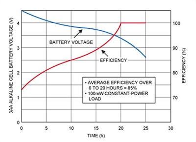
Figure 1: Linear regulator efficiency vs. battery voltage in a system using three AA sized alkaline batteries (at 100 mW constant power load); notice how the regulator’s efficiency increases toward the dropout voltage. (Image source: Maxim Integrated)
Although the efficiency with fully charged batteries is around 73%, the average efficiency across the discharge cycle is 85%. That’s the number that should be compared with the equivalent figure for a switching regulator, and the efficiency of which won’t increase as the battery voltage falls.
Again, referring to Figure 1, we see that after 20 hours while the batteries still have some charge, the difference in input and output voltages is too small for the device to regulate and it ceases to operate. In total, the cumulative amount of battery energy that has been used to actually power the product is:
Average regulation efficiency × battery energy percentage used before failure =
85% × 80% = 68%.
Selecting an IC with a lower dropout voltage capability ensures more of the battery’s charge is used up, and hence, improves efficiency.
“Dropout” is defined as the difference between the input and output voltage just before regulation ceases. For the example shown in Figure 1, if the linear regulator is swapped for a device with an improved dropout voltage (from 3.4 to 3.0 volts), an extra 2.5 hours can be extracted from the batteries and the battery energy usage improves to:
85% × 90% = 76.5%
Check the manufacturers’ datasheets very carefully because some so-called “low-dropout” (LDO) devices can feature input/output voltage differences that are quite large. That can mean the lights go out while the batteries still hold a lot of charge. Note that the dropout voltage will vary depending on the load current.
LDO selection and implementation
The design engineer looking to select an LDO and therefore take advantage of a linear regulator’s advantages for certain applications can easily be overwhelmed by the many available choices. Despite their apparent simplicity, the data sheet for a typical LDO will often have twenty, thirty and even more performance graphs in addition to the basic specifications table. These graphs show both static and dynamic behavior, as well as capabilities over various operating scenarios and conditions.
Among the LDO devices for portable applications, there are dozens of devices to suit a wide range of input and output voltages. Some have fixed output voltage, some have user adjustable outputs, and some can deliver a negative output rail. Some LDOs are relatively general purpose and have alternate sources, while others are optimized in one or more of their parameters and thus target specific application niches. A few examples illustrate the variety of available LDOs.
Automotive: Maxim Integrated’s MAX16910 is a 200 mA, ultra-low quiescent current LDO for automotive applications. In addition to its basic performance, it is qualified for the extremely stringent demands of the automotive environment. Its input is tolerant of transients to +45 volts, it can withstand and operate under automotive “load-dump” conditions, and it can function (and is specified) over the -40°C to +125°C automotive temperature range (Figure 2). It operates from a +3.5 volt to +30 volt input, yet consumes only 20 microamps (µA) of quiescent current at no load, and only 1.6 μA when in user controlled shutdown mode.
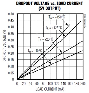
Figure 2: Maxim Integrated’s MAX16910 is noteworthy because it meets the stringent automotive requirements for guaranteed functionality along with fully specified operation from -40°C to +125°C. (Image source: Maxim Integrated)
Negative voltage: When designing for a negative voltage, it is not simply a matter of using the converter connected “upside down” as there will be ground reference issues and other topology problems. Instead, a negative specific LDO is needed. The ADP7183 series from Analog Devices features both a negative input/output and ultralow noise (Figure 3).
These ICs operate from an input of −2.0 volts to −5.5 volts, and deliver a maximum output current of −300 milliamps (mA). They offer a choice of 15 fixed output voltage options from −0.5 volts to −4.5 volts, or with an adjustable output from −0.5 volts to −VIN + 0.5 volts. In addition, output noise is just 4 μVRMS from 100 Hz to 100 kHz, and noise spectral density is 20 nV/√Hz from 10 kHz to 1 MHz. Finally, the typical power supply rejection ratio (PSRR) is 75 dB at 10 kHz; 62 dB at 100 kHz; and 40 dB at 1 MHz.
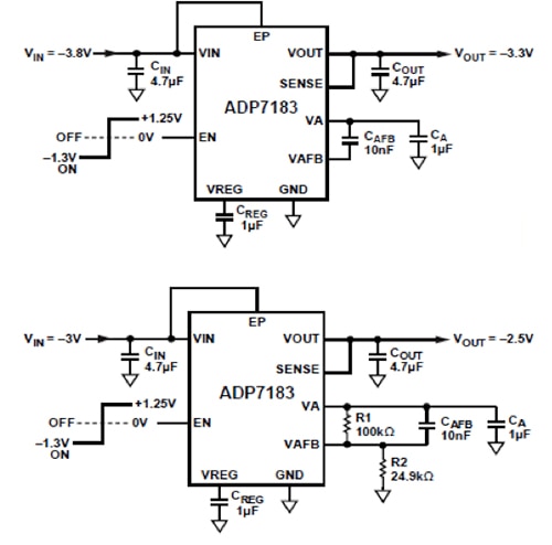
Figure 3: The ADP7183 series from Analog Devices is for negative source/negative output applications, which actually occur fairly often; these devices can be configured for fixed output (here, −3.3 volts in the upper schematic) or a user-adjustable output (here, set to −2.5 volts, lower schematic). (Image source: Analog Devices)
Fixed/variable dual output: For applications that need more than a single LDO, which is a fairly common situation, Texas Instruments offers the LFC789D25 dual linear controller with one fixed output at 2.5 volts and one adjustable output. The controller’s outputs are designed to drive external N-channel MOSFETs, so currents can be relatively high, up to 3 A (typical). This IC targets applications such as DDR1 memory voltage (VDDQ) and VREF buffer (Figure 4). Its internal reference provides temperature compensated performance with a tolerance of 2%, which is adequate for the situation.
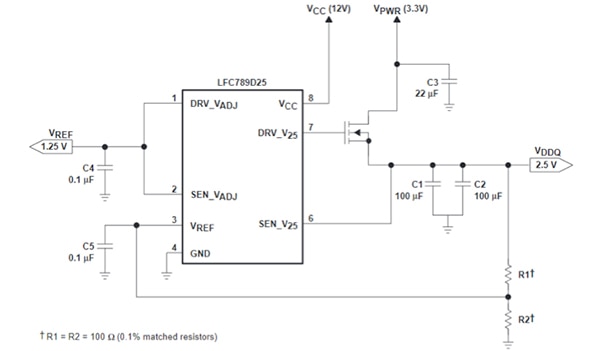
Figure 4: Texas Instruments’ LFC789D25 dual linear controller, with one fixed and one adjustable output, meets the needs of important applications niches, such as DDR1 and similar memory arrays. (Image source: Texas Instruments).
Near-zero quiescent current: For battery powered applications where miserly use of available energy is critical to meeting runtime objectives, the Richtek RT9069 family features an ultralow quiescent current (Iq) of just 2 µA. Their enable pin can put these ICs into a deep sleep state where the quiescent current is zero.
These LDOs operate over a wide input range from 3.5 volts to 36 volts, delivering up to 200 mA. They are available with fixed output voltages of 2.5, 3.3, 5, 9, and 12 volts. They are stable over the entire input voltage range and output current range using just a single ceramic output capacitor, in addition to the standard input filter capacitor which most LDOs require (Figure 5).
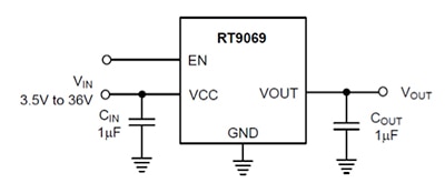
Figure 5: The Richtek RT9069 series is designed for maximizing run time in severely constricted battery powered applications, with quiescent current of just 2 µA, and zero quiescent current when directed to its disabled state. (Image source: Richtek Technology Corp.)
Getting the most from an LDO
While LDOs are fairly simple to use, some basic guidelines must be respected in order to realize their benefits and avoid potential damage. These include the issues of practical design such as thermal concerns and packaging, layout considerations, and noise pickup.
For thermal issues, it is essential to study the data sheet table and graph for safe operating area and derating (Figure 6).
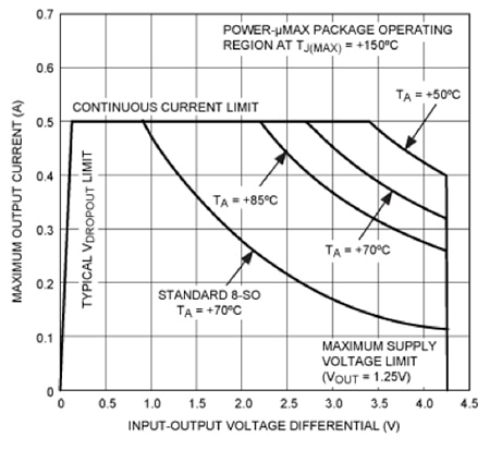
Figure 6: For an LDO, the safe operating area has an inverse relationship between the maximum allowable output current and the magnitude of the input-output voltage differential; also, package type plays a large role as shown by the difference between the standard SO-8 and proprietary 8-pin µMAX packages. (Image source: Maxim Integrated)
The derating is a function of many variables, including the LDO package. A 5-pin SOT-23 package is typically rated for over 500 mW dissipation, while some exposed pad packages are rated for almost four times that value. If the LDO is situated in an optimal setting with sufficient airflow and/or a low impedance thermal path, defining the derating performance due to self-heating will be straightforward using the vendor data.
Conclusion
Linear regulators have the advantage of very "clean" output with little noise introduced into their DC output, but they can be much less efficient than switching converters and are unable to step-up the input voltage like their switched counterparts.
Nonetheless, there are applications where the linear regulator is the preferred and “best” choice of DC/DC converter topology in terms of simplicity, cost, and under certain operating conditions, efficiency.
References
- “Linear Regulators in Portable Applications,” Application Note 751, Maxim Integrated
- “Understanding the Efficiency of an LDO,” Texas Instruments

Disclaimer: The opinions, beliefs, and viewpoints expressed by the various authors and/or forum participants on this website do not necessarily reflect the opinions, beliefs, and viewpoints of DigiKey or official policies of DigiKey.


