Transistor Basics: NPN & PNP Using 2N3904, 2N3906, 2N2222, and 2N2907
Contributed By DigiKey
2017-12-21
Amazingly, the first operational Transistor was declared 70 years ago, on December, 23 1947!1 The Transistor is probably one of the most revolutionary components ever invented. It led the way for the creation of integrated circuits, microprocessors and computer memory.
In this article, we'll discuss the following areas;
(click the link to skip to any section that suits your needs)
- What is a transistor?
- How does a transistor work?
- Choosing a transistor for your application
- Transistor circuit examples
- History Behind the invention of the transistor
- Reference links for further study
What is a transistor?
A transistor, also known as a BJT (Bipolar Junction Transistor), is a current driven semiconductor device which can be used to control the flow of electric current in which a small amount of current in the Base lead controls a larger current between the Collector and Emitter. They can be used to amplify a weak signal, as an oscillator or as a switch.
They are usually made of silicon crystal where N & P type semiconductor layers are sandwiched together. See Figure 1 below.
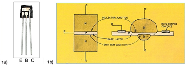
Figure 1: Figure 1a shows a 2N3904 TO-92 cut-away revealing E - Emitter, B - Base, and C – Collector leads tied to Silicon. Figure 1b is taken from a May 1958 Radio-Electronics Magazine2 showing the N & P type layer slices and arrangements (referenced as Germanium material at that time).
Transistors are hermetically sealed and encased in plastic or a metal can with three leads (Figure 2).
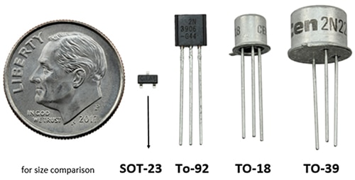
Figure 2: A size comparison and a variety of popular package types.
How does a transistor work?
For an example, we will show how an NPN transistor works. A simple way to view its function as a switch is to think of water flowing through a tube controlled by a Valve. Water pressure represents ‘Voltage’ and water flowing through a tube represents ‘Current’ (Figure 3). The large tubes represent the Collector/Emitter junction with a Valve in-between, expressed in the figure as a Gray Oval, like a moveable flap, which is actuated by current from a small tube representing the Base. The valve keeps the water pressure from flowing from Collector to the Emitter. When water flows through the smaller tube (the Base), it opens the valve between the Collector/Emitter junction, allowing water to flow through to the Emitter, and on to Ground (Ground represents the return for all water or Voltage/Current).
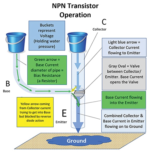
Figure 3: This graphical representation illustrates how a transistor functions. When water flows through the smaller tube (Base), it opens the valve between the Collector/Emitter junction, allowing water to flow through the Emitter to Ground.
Choosing a transistor for your application
If you want to simply turn on a circuit or switch on a load, there are certain things you should consider. Determine if you want to bias or energize your transistor switch with positive or negative current (i.e. NPN or PNP type, respectively). An NPN transistor is driven (or turned on) by positive current biased at the base to control the current flow from Collector to Emitter. PNP type transistors are driven by a negative current biased at the base to control the flow from Emitter to Collector. (Note that polarity for PNP is reversed from NPN.) See Figure 4 below for more details.
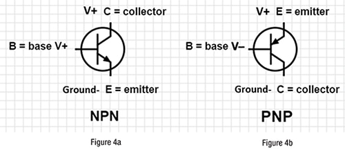
Figure 4: Schematic Symbols for each type of transistor.
After the bias voltage is determined, the next variable that is needed is the amount of voltage and current the load requires to operate. These will be the minimum voltage and current ratings of the transistor. Tables 1 and 2 below show some popular transistors and key specifications including their voltage and current limits.
 Transistors, NPN and PNP, Leaded and Surface Mount
**Specifications may vary - verify details in datasheet |
||||||||||||||||||||||||||||||||||||||||||||||||||||||||||
Table 1. Popular leaded and surface mount NPN and PNP transistors.
 Transistors, NPN and PNP, Metal Can Packages
|
||||||||||||||||||||||||||||||||||||||||||
Table 2. Popular metal can packaged NPN and PNP transistors.
Transistor circuit examples
Figure 5 below shows a circuit example which turns on the Collector-Emitter junction by energizing the Base, or biasing the transistor to turn it on, by bringing 5 volts to the base via a slide switch. This example lights an LED which is the load in this case. The proper use of resistors to prevent overcurrent draw is required when biasing the base. I used leaded parts in a bread board to test my example circuit. Most engineers will use surface mount components (much smaller size than a TO-92 package) when it comes to using transistors in a new product design going to market. Here is a link that shows various package sizes for 3904 transistors.
Since the 2N3904 is an NPN transistor, the base needs positive biasing (appropriate voltage levels and resistance) to turn on the collector emitter junction for proper current flow. Use of a load resistor (R1) is also important so there is not too much current being driven through the LED and transistor. For more information on this transistor, see the 2N3904 datasheet.
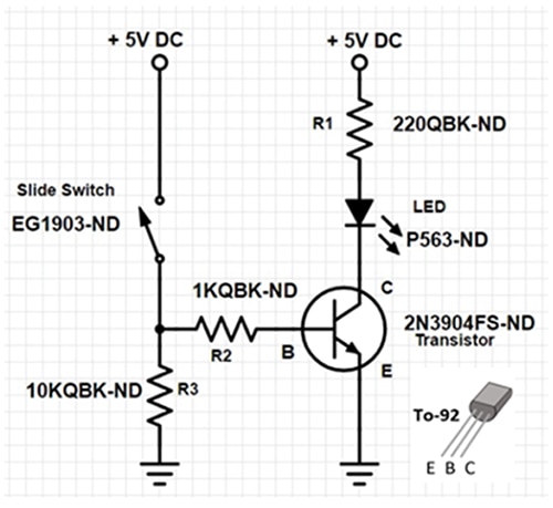
Figure 5: 2N3904 circuit example for lighting an LED with a EG1218 slide switch showing pins C (Collector), E (Emitter), and B (Base) (Image drawn in Scheme-it).
Figure 6 is an example night light circuit using a PNP transistor. To see the details of this circuit, link over to DigiKey’s engineering wiki site and search PNP Night Light.
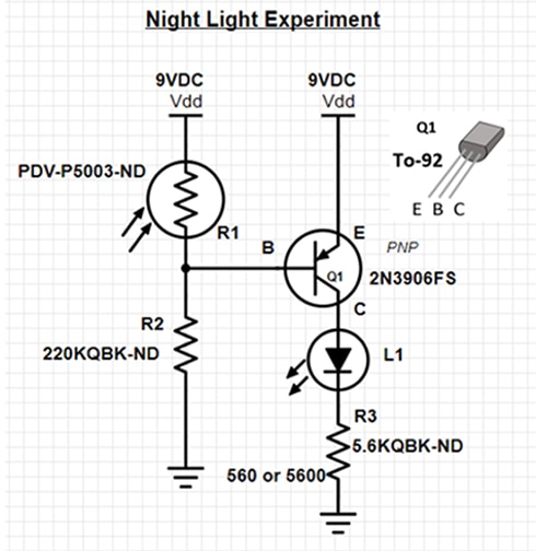
Figure 6: 2N3906 example night light circuit for lighting an LED with a PDV-P5003 photocell (Image drawn in Scheme-it)
Brief history of the invention of the transistor
How did it all start? This rabbit hole goes very deep; however, I’ll start with the invention of the telephone. Many would argue who truly invented the first working electrical prototype; however, the first patent was obtained by Alexander Graham Bell on March 7th, 18763, and he later formed the American Telephone and Telegraph company (aka AT&T). Right around 18941 Bell’s patent expired. Although AT&T dominated the telephone market up to the early 1900s, other companies formed and were taking customers away from AT&T. Because of this, the company felt the need to continue to dominate and expand their market. In 1909, AT&T President Theodore Vail1 wanted to transmit phone calls transcontinental (New York to California). But to do this they needed a good amplifier or repeater to boost the signals traveling long distances. Previously in 1906, Lee De Forest had taken an idea created by John A. Fleming (who took work from Thomas Edison, creating a vacuum tube device called the “oscillation valve” used to detect radio waves), modified it to create the Triode – an inefficient 3 terminal vacuum tube that could be used as an amplifier. In 1912 Forest was invited by Harold Arnold of Western Electric Company (AT&T’s manufacturer) to show off his invention. Although Forest’s Triode worked at low voltages, Arnold needed it to work at higher voltages to make effective repeaters for transmitting voice over long distances. Arnold believed he could make a better Triode and so he hired scientists to understand how the device worked and how he might improve it. In October 1913, he was successful. Soon after that telephone lines were installed everywhere. The investments that AT&T made hiring top scientists over the years made them realize doing deep research would give them a competitive advantage over their competition and so formed the “Bell Telephone Laboratories” in 1925.
Many thousands of vacuum tubes and relays were needed to keep the telephone lines running. However, vacuum tubes took a lot of power, were large, and burned out frequently. Gaining an understanding from World War 2 technology developments of the crystal rectifier used to enable radar, Mervin Kelly, Bell’s Director of research, had an inkling that semiconductors (solid-state devices) may be the answer to creating a device that could replace the expensive, unreliable vacuum tubes. Kelly sought out one of their brilliant physicists, William Shockley, to explain his vision of improving the components used to transfer voice over wires. Kelly expressed his feelings that he would be glad when noisy mechanical relays and power hungry vacuum tubes would someday be replaced by solid-state electronic devices. This really stuck well with Shockley and became his primary goal. Kelly put Shockley in charge of finding a way to make it happen.
He was a brilliant theorist but not so good at constructing his ideas. Shockley had made several attempts to try proving an idea he had of the field effect transfer of electrons to connect two sides of a semiconductor by energizing a plate above the semiconductors. He was unsuccessful. Frustrated, he turned to two other physicists at Bell labs, John Bardeen (brilliant with electron theory in semiconductors) and Walter Brattain (great with prototype & use of lab equipment). They became part of his team. Shockley allowed the dual team to work on their own. Over the years, many attempts were made trying to get the field effect work but it never did. They went over their calculations and in theory it should have worked. Thinking out of the box, Bardeen and Brattain experimented with thin slices of silicon and germanium trying to get the field effect to work. In the fall of 1947 there was a sign of progress as Brattain was having trouble with condensation of water settling on the surface of the semiconductor. Rather than drying it out he placed a drop of water on top of the silicon, energized the plate above it, and noticed an amplifying effect. The water drop helped overcome the surface barrier which helped create the electron flow, but it was sluggish and not able to cleanly amplify voice signals that would be needed to successfully transmit voice.
In December of 1947 (noted as the Miracle Month) they thought of eliminating the gap of field effect, removing the water and creating a gold contact to touch the semiconductor. They switched to germanium, which was easier to work with at that time, and isolated it with a thin oxide film which naturally forms on germanium. Many tests were done with no success. Then in mid-December, apparently by accident, Walter Brattain had inadvertently washed off the oxide coating, making the gold contact direct to the germanium! Bingo!!! He had discovered good amplification and the Transistor was functional. Instead of electrons being pulled to the surface of the semiconductor as theorized by Shockley’s field effect idea, Brattain/Bardeen had discovered that by contacting the semiconductor with a gold contact, they were injecting holes into the semiconductor, enabling the electricity to flow. Around mid-December 1947, without Shockley’s knowledge they began creating an operational prototype. Brattain put together an apparatus in the shape of a plastic triangle with gold foil along the slanted edges and made a razor thin slit at the triangle point. It was an extremely crude prototype. They used a paper clip made into a spring to press the triangle into the thin germanium semiconductor, on top of a thin copper plate, where there were two leads – one on each end of the triangle. The copper plate under the germanium slice served as the 3rd lead, if you will (Figure 7). It ended up being called the Point Contact Transistor.
Brattain and Bardeen called Shockley to let him know the good news. What I’ve researched says Shockley had mixed emotions, glad that it was functional but disappointed that he did not directly create it. The demonstration to Shockley’s bosses came a week after they discovered it on December 23rd, 1947 (it was publicly announced on June 30, 1948). Later, a picture was taken at that time for history (Figure 8). Shockley knew the fragile point contact transistor would not be easy to manufacture and he was consumed by trying to make it better (by himself). Shockley worked feverishly to try to solve the problem his way… documenting his thoughts of trying to make it more integrated by layering the semiconductor materials together. Much more research was involved to complete the theory for filing a patent for the junction transistor (filed June 25th, 1948). A functional n-p-n junction transistor was demonstrated on April 20th, 1950 (enabled by the work of Gordon Teal and Morgan Sparks). The details around all of this goes much deeper than you can imagine4.
The Nobel prize for the invention of the Transistor effect was given to William Shockley, John Bardeen, and Walter Brattain on December 10, 1956.
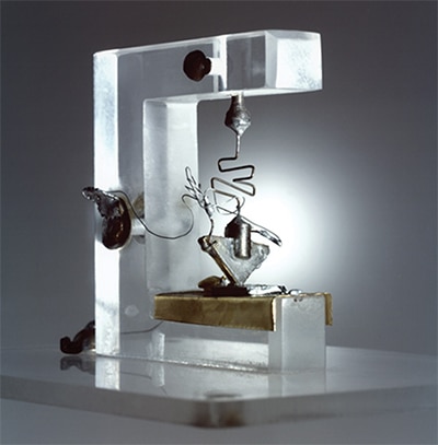
Figure 7: The Point Contact Transistor (Reused with permission of Nokia Corporation)
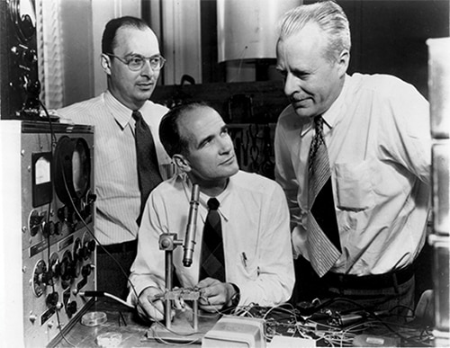
Figure 8: John Bardeen, left, William Shockley, middle, and Walter Brattain, right. (Reused with permission of Nokia Corporation)
References
- Riordan, Michael and Lillian Hoddeson. 1997. Crystal Fire: The Invention of the Transistor and the Birth of the Information Age. New York, NY: W.W. Norton & Company, Inc.
- Ryder, R.M. 1958. “Ten years of Transistors”, Radio-Electronics Magazine, May, page 35.
- Houghton Mifflin Harcourt Publishing Company. 1991. “ALEXANDER GRAHAM BELL”. Retrieved Dec. 19, 2017.
- Riordan, Michael, Lillian Hoddeson, and Conyers Herring. 1999. “The Invention of the Transistor”, Modern Physics, Vol 71, No. 2: Centenary.
Additional information can be found at: http://www.pbs.org/transistor/

Disclaimer: The opinions, beliefs, and viewpoints expressed by the various authors and/or forum participants on this website do not necessarily reflect the opinions, beliefs, and viewpoints of DigiKey or official policies of DigiKey.


