The Basics of Voltage Controlled Oscillators (VCOs) and How to Select and Use Them
Contributed By DigiKey's North American Editors
2021-01-26
Many electronic applications require that a signal’s frequency be varied based on the amplitude of another signal. A good example is a frequency modulated signal where the frequency of a carrier varies with the amplitude of the modulation source. Also consider a phase locked loop (PLL): This uses a control system to vary the frequency and/or phase of an oscillator to match the frequency/phase of an input reference signal.
The goal for designers is to determine how to perform this function as efficiently and cost-effectively as possible, while ensuring accuracy, reliability, and stability over time and temperature.
This is the function of voltage controlled oscillators (VCOs). These devices are designed to produce an output signal whose frequency varies with the voltage amplitude of an input signal over a reasonable range of frequencies. They are used in PLLs, frequency and phase modulators, radar and many other electronic systems.
This article explains why VCOs are so often a designer’s best choice for this function and then briefly describes how VCOs work, and the design of VCOs from discrete component designs to monolithic VCO ICs. It then looks at how VCOs can be specified to match specific applications using real-world examples from various vendors, including Maxim Integrated, Analog Devices, Infineon Technologies, NXP Semiconductors, Skyworks Solutions, and Crystek Corporation.
What is the role of a VCO?
As mentioned, many electronic applications require that a signal’s frequency or phase be varied or controlled based on the amplitude of another signal. Typical applications include communications systems, frequency chirps in radar, phase tracking in PLLs, and frequency hopping applications such as remote keyless entry (Figure 1).
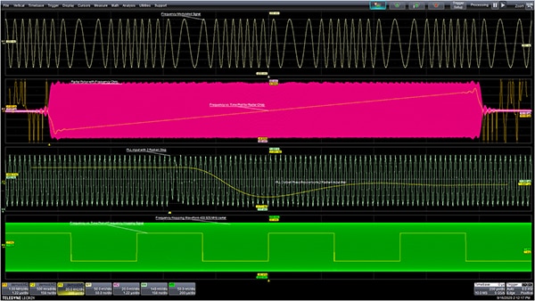 Figure 1: Examples of applications that require variations in frequency or phase controlled by an applied signal voltage include frequency modulation in communications systems (top), frequency chirps in radar (second down), phase tracking in phase locked loops (third down), and frequency hopping applications like remote keyless entry systems (bottom). (Image source: DigiKey)
VCOs are specifically designed to produce an output signal whose frequency varies according to the amplitude of an input signal over a reasonable range of frequencies.
How VCOs work
VCOs come in discrete, modular, and monolithic forms, but a discussion of discrete VCOs will provide a basic understanding of how they operate and why certain specifications matter. An overview of modular and monolithic solutions will follow.
Using a discrete approach to VCOs, designers have a great deal of flexibility with respect to satisfying custom specifications. This approach is especially common with do-it-yourself (DIY) projects, particularly in amateur radio. Such designs, intended for operation in high-frequency radio projects, are based on classic oscillator topologies including the Hartley and Colpitts inductor-capacitor (LC) oscillators (Figure 2).
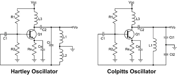 Figure 2: Classic oscillators, including the Hartley and Colpitts LC oscillators, can be used as the basis of a VCO design. (Image source: DigiKey)
All oscillators are based on the use of positive feedback to achieve sustained oscillation. The Hartley and Colpitts oscillators are basic designs that generate positive feedback in different ways. Positive feedback requires that the signal at the oscillator’s output be returned to the input with a total phase shift of 360°. The amplifier provides a single-phase inversion of 180°, and the other half of the 360° comes from the LC of the resonant tank circuit. The tank circuit determines the nominal frequency of oscillation. It consists of L1, L2, and Ct in the Hartley oscillator circuit, and L1, Ct1 and Ct2 in the Colpitts oscillator.
The Hartley oscillator uses inductive coupling to obtain the phase reversal by means of a dual or tapped inductor (L1 and L2) shown in the circuit. The Colpitts oscillator employs a capacitive voltage divider consisting of Ct1 and Ct2 in the respective circuit. There are many designs derived from these basic designs, each with its own name. The derivative designs attempt to isolate the tank circuit from the amplifier to prevent frequency shifts due to loading. There are many such derivatives from which designers can pick their favorite.
Frequency control is added to these designs by employing varactor diodes to vary the resonant frequency of the tank circuit. The varactor diode, sometimes called a varicap diode, is a junction diode designed to provide variable capacitance. The P-N junction is reverse biased and the diode capacitance can be varied by changing the applied DC bias. The capacitance of the varactor varies inversely with the applied DC bias: the higher the reverse bias, the wider the diode depletion region, and hence the lower the capacitance. This variation can be seen in the capacitance vs. reverse voltage graph for the Skyworks Solutions SMV1232_079LF hyper-abrupt junction varactor diode (Figure 3). This diode has a capacitance of 4.15 picofarads (pF) at zero volts and 0.96 pF at 8 volts.
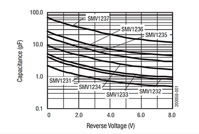 Figure 3: The voltage-capacitance plot of the Skyworks Solution SMV1232 varactor diode shows clearly how the capacitance varies inversely with the applied DC bias. (Image source: Skyworks Solutions)
The capacitance range of the varactor diode determines the tuning range of the VCO. Voltage control of the oscillator is realized by adding the varactor in parallel with the tank circuit, as shown in Figure 4. The figure shows an evaluation board reference design of a Colpitts oscillator VCO with a center frequency of 1 gigahertz (GHz) and a tuning range of about 100 megahertz (MHz). It incorporates an emitter follower buffer to isolate the VCO from load variations. The resonant tank circuit in this design includes the inductor L3 and the capacitors C4, C7, and C8. The varactor diode, VC1, is in parallel with the tank. Capacitor C4 controls the range of frequency variation for a given varactor selection, while C7 and C8 provide the required feedback to maintain oscillation.
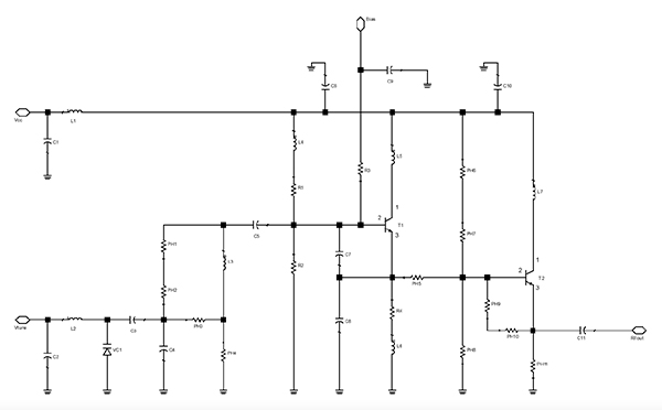 Figure 4: An evaluation board reference design of a Colpitts oscillator VCO with a center frequency of 1 GHz and a tuning range of about 100 MHz. The varactor diode, VC1 (lower left), is in parallel with the tank, comprising inductor L3 and the capacitors C4, C7, and C8. (Image source: NXP Semiconductors)
The choice of the varactors and the bipolar junction transistors depends on the frequency of the oscillator. For nominal frequencies of 1 GHz, RF transistors such as NXP Semiconductor’s BFU520WX or Infineon Technologies’ BFP420FH6327XTSA1 can be used. The BFU520WX has a transition frequency of 10 GHz and gain of 18.8 decibels (dB), and the BFP420FH6327XTSA1 has a transition frequency of 25 GHz with a gain of 19.5 dB. Both have a sufficient gain-bandwidth product for this circuit at 1 GHz.
In sum, discrete VCOs offer maximum design flexibility but are larger and take up more pc board area than modular or monolithic devices.
Specifying VCOs
The principal VCO specifications usually begin with the nominal frequency range, meaning the minimum and maximum frequencies obtainable. Alternatively, they might be specified as a nominal or center frequency and a tuning range.
The input tuning voltage range corresponds to the input voltage swing, which tunes the VCO over the tuning range (Figure 5).
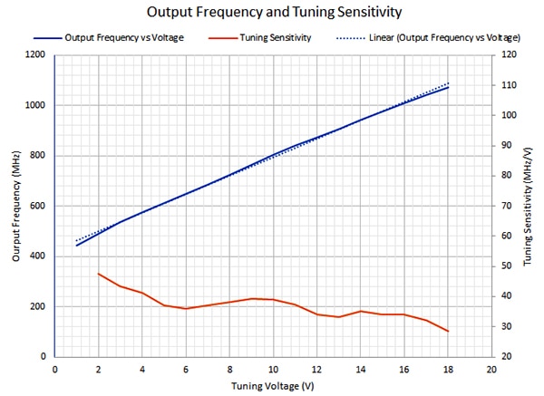 Figure 5: The tuning curve plot of output frequency as a function of input tuning voltage provides a basic view of the linearity of the VCO compared to a linear fit. The slope of the output frequency vs. tuning voltage is the tuning sensitivity. (Image source: DigiKey)
The tuning gain or sensitivity, measured in units of MHz/volt (V), is the slope of the frequency vs. voltage plot. It is a measure of the tuning linearity. In applications where the VCO is in a control loop such as with a PLL, the tuning sensitivity is the gain of the VCO element and may affect the dynamics and stability of the control loop.
The output power of the VCO specifies the power delivered to a load of specified impedance, usually 50 ohms (Ω) for RF VCOs. Output power is specified in dB referenced to 1 milliwatt (mW) (dBm). The flatness of the power output over the frequency range of the VCO may also be of interest.
Load pulling is the change in the VCO’s output frequency due to changes in load impedance measured in MHz peak to peak (pk-pk). Load isolation is usually improved by using a buffer amplifier like the emitter follower shown in Figure 4.
Power supply pushing is the variation in VCO output frequency due to variations in the power supply voltage. It is measured in MHz/V.
The phase noise specification is an indicator of the VCO’s signal purity. An ideal oscillator has a frequency spectrum that is a narrow spectral line at the oscillator’s frequency. Phase noise represents unwanted modulation of the oscillator and broadens the spectral response. Phase noise is the result of thermal and other noise sources within the oscillator circuit and is given as decibels below the carrier per hertz (dBc/Hz). Phase noise in the frequency domain results in timing jitter in the time domain manifested as time interval error (TIE).
Modular VCOs
Modular VCOs represent the next highest level of circuit integration. These VCOs are packaged in a small modular enclosure and are used like a component. Modular VCOs generally offer higher packing density than a discrete implementation of a VCO. They are available in a range of output frequencies, tuning ranges, and power output levels. An example is Crystek Corporation’s CRBV55BE-0325-0775 VCO (Figure 6). This device measures 1.25 x 0.59 inches (in.) (31.75 x 14.99 millimeters (mm)) with a height of 1.25 in. and has a tuning range of 325 to 775 MHz for an input voltage range of 0 to 12 volts. It has an output power level of +7 dBm (typical) with a phase noise of -98 dBc/Hz @10 kilohertz (kHz) offset from the carrier, and -118 dBc/Hz at 100 kHz.
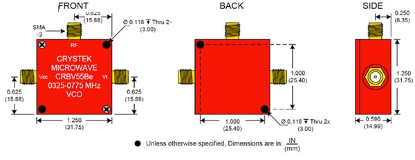 Figure 6: Outline drawings for the Crystek CRBV55BE VCO showing its compact form factor with dimensions of 1.25 x 1.25 x 0.59 in. (Image source: Crystek Corporation)
As for control dynamics, the Crystek VCO has a typical tuning sensitivity of 45 MHz/V. Power supply pushing is specified as 0.5 MHz/V typical and 1.5 MHz/V maximum. Load pulling is 5.0 MHz pk-pk, maximum.
Monolithic VCOs
VCOs can be implemented as monolithic ICs. The monolithic IC provides the highest volume density. Like modular VCOs, monolithic VCOs are designed for specific operational bands. As an example, consider the Maxim Integrated MAX2623EUA+T. This is a self-contained VCO with an integrated oscillator and an output buffer in a single 8-pin mMax package (Figure 7).
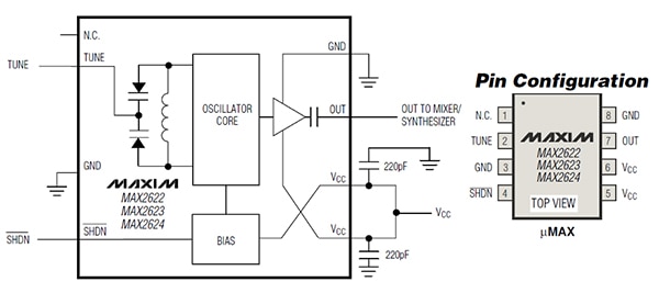 Figure 7: The block diagram and pin configuration of the Maxim Integrated MAX2623 VCO. It is a conventional LC based VCO using dual varactor diodes for voltage control. It includes a built-in output buffer in an 8-pin package. (Image source: Maxim Integrated)
The design includes an on-chip tank inductor and varactor diodes. It operates with a +2.7 to +5.5 volt power supply and draws only 8 milliamperes (mA). The MAX2623 is one of three VCOs in the product family, each of which is differentiated by their intended operating frequencies. The MAX2623 is tuned to the 885 to 950 MHz range, which covers the 902 to 928 MHz Industrial, Scientific and Medical (ISM) band, where it can be used as a local oscillator. The VCO has an output power level of -3 dBm into 50 Ω with phase noise of -101 dBc/Hz typical at 100 kHz offset. The control voltage range is 0.4 to 2.4 volts, and load pulling is typically 0.75 MHz, pk-pk. Power supply pushing is 280 kHz/volt (typical). Its package measures 0.12 x 0.12 x 0.043 in. (3.03 x 3.05 x 1.1 mm).
Another example of a monolithic VCO is Analog Devices’ HMC512LP5ETR. This VCO covers the frequency range of from 9.6 to 10.8 GHz using a tuning voltage of from 2 to 13 volts. It is intended for satellite communications, multipoint radio, and military applications (Figure 8).
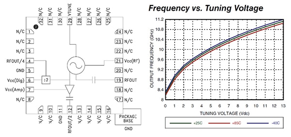 Figure 8: The block diagram of the Analog Devices HMC512LPETR VCO showing the integrated varactor diode and the oscillator core with integrated resonator. (Image source: Analog Devices)
This monolithic microwave integrated circuit (MMIC) VCO uses GaAs and InGaP heterojunction bipolar transistors to achieve wide bandwidth and an output power level of +9 dBm into a 50 Ω load using a 5 volt DC power source. Phase noise is -110 dBc/Hz at 100 kHz offset. Load pulling is typically 5 MHz peak to peak typical. Power supply pushing is typically 30 MHz/volt typical at 5 volts. The device is packaged in a QFN 5 x 5 mm surface mount package. Note in the figure that this VCO also includes half and quarter-frequency auxiliary outputs. These fractional frequency outputs can be used for driving a PLL synthesizer to phase lock the VCO primary output if desired, or to synchronize other timing chain signals.
Both of these monolithic devices feature small size, which is the primary advantage of this type of VCO.
Conclusion
VCOs, whether in discrete, modular, or monolithic form, fill the need for voltage-based frequency control that is required in a number of applications. They are used in function generators, PLLs, frequency synthesizers, clock generators and analog music synthesizers. While they are relatively simple devices, their proper use requires a solid understanding of how they operate and their key specifications. Once those are clear, there are many designs and vendors from which to choose.

Disclaimer: The opinions, beliefs, and viewpoints expressed by the various authors and/or forum participants on this website do not necessarily reflect the opinions, beliefs, and viewpoints of DigiKey or official policies of DigiKey.


