Simplify Precision Impedance Analyzer Design with a System-on-Module Approach
Contributed By DigiKey's North American Editors
2024-09-10
Many applications require precise impedance measurements, including touch panel calibration, semiconductor characterization, wafer acceptance, and battery testing. Automated test equipment (ATE) for these applications typically needs to measure impedance over a wide frequency range with high accuracy and sensitivity.
Developing a custom impedance measurement device for these applications involves numerous challenges, including hardware design, software development, and testing. These parameters require substantial analog and digital signal processing expertise and can cause delays that may jeopardize a project’s schedule and budget.
To circumvent these challenges, designers can select a system-on-module (SOM) that pre-integrates the critical hardware and software needed for high-precision impedance measurements. Such a module allows designers to focus on their core competencies and application-specific development rather than the intricacies of impedance-measurement technology.
This article briefly reviews the key requirements for impedance measurement in ATE. It then introduces a suitable impedance analyzer SOM from Analog Devices Inc. (ADI) and demonstrates how to use the module with its associated evaluation board.
Requirements for precision impedance measurement in ATE
ATE for applications such as touch panel calibration, semiconductor characterization, wafer acceptance, and battery testing has specific requirements that include:
- Wide frequency range capability, often from under 1 hertz (Hz) to megahertz (MHz)
- High accuracy and consistency, typically 0.1% or better
- High sensitivity to measure small impedance changes
- Fast measurement speeds for high-throughput testing
- The ability to handle a wide range of impedance values, from microohms (µΩ) to megaohms (MΩ)
- Automated sweeps and complex measurement sequences capability
It is worth noting that the requirements can vary considerably between applications. For example, touch panel calibration may require sensitivity to capacitance changes in the femtofarad (fF) range, while wafer acceptance sensitivity can reach the attofarad (aF) range.
Challenges of designing precision impedance measurement for ATE
Developing ATE for these applications involves substantial expertise and resources, which can lead to long development cycles and high non-recurring engineering costs. Challenges related to custom impedance measurement design include the following:
- Complex hardware design: Creating high-precision analog front-ends capable of accurate measurements across a wide frequency range and impedance range requires expertise in analog and digital signal processing and careful attention to printed circuit board (pc board) layout and shielding details.
- Sophisticated software development: Implementing impedance calculation, calibration, and compensation algorithms is complex. Supporting multiple measurement formats and automated sweeps adds further intricacy.
- Calibration and accuracy: Achieving and maintaining high accuracy across different measurement conditions requires sophisticated calibration procedures and compensation techniques.
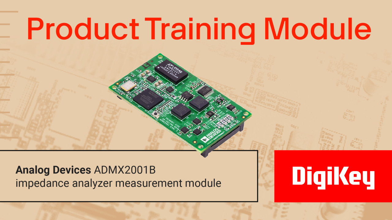
A pre-engineered evaluation module such as ADI’s ADMX2001B can significantly simplify these challenges. This SOM integrates the main components of a precision impedance analyzer into a compact 1.5 x 2.5 inches (in.). As illustrated in Figure 1, the module plugs into the EVAL-ADMX2001EBZ evaluation board, which comes with design exploration and rapid prototyping software.
 Figure 1: The ADMX2001B impedance measurement module plugs into the EVAL-ADMX2001EBZ evaluation board. (Image source: Analog Devices)
Although the module is not intended for production designs, the schematic, bill of materials (BOM), Gerber files, and firmware are available. This enables companies to either build their own version of the module or integrate it into a larger design. Either way, the pre-engineered design offloads many challenging tasks, allowing companies to focus on their specialized areas.
Creating a module is a particularly interesting option, giving developers a straightforward, cost-effective path to scale their design. When adding features or adapting the design for different use cases, developers can retain the module as their design core rather than starting from scratch.
ADMX2001B feature and performance overview
The ADMX2001B combines high-performance mixed-signal circuitry and advanced processing algorithms for precise impedance measurements. The module offers a versatile frequency range from DC to 10 MHz and a high measurement accuracy of 0.05%. It covers a broad resistance range from 100 µΩ to 20 MΩ, capacitance from 100 aF to 160 F, and inductance from 1 nanohenry (nH) to 1600 henrys (H). It can perform measurements at a rate of typically 35 milliseconds (ms) per measurement, and it provides 18 impedance measurement formats that cater to various applications and component types.
Automated features, including multi-point and parametric sweeps and DC resistance measurements, enable the ADMX2001B to perform complex sequences and thorough component characterization without manual intervention. Automated calibration routines, non-volatile memory, and compensation features ensure measurement traceability, reliability, and the elimination of fixture parasitics. The module’s compact size with UART, SPI, and GPIO interfaces allows easy integration into high-density test systems and portable equipment. Additionally, it supports development on Windows, macOS, Linux, Raspberry Pi, and Arduino platforms, making it adaptable to larger systems or custom applications.
These capabilities make the module suitable for a wide variety of demanding applications.
Overview of the EVAL-ADMX2001EBZ evaluation board
Developers can use the EVAL-ADMX2001EBZ evaluation and development breakout board to explore design ideas with the ADMX2001B. This board provides convenient access to the functionality of the module and features:
- BNC connectors that can interface to common inductance, capacitance, resistance (LCR) meter test probes and fixtures
- UART interface that can be used with USB-to-UART cables to interface to the host PC
- Trigger and clock synchronization signals available through SMA connectors that simplify the connection to standard test equipment
- Arduino-style headers that allow the user to develop embedded code with boards such as the SDP-K1
- A power jack that accepts various input voltages from AC/DC power adapters that can supply 5 volts to +12 volts
The primary purpose of the evaluation board is to provide an LCR meter demo. To perform this demonstration, additional hardware is needed:
- LCR meter accessories, such as test fixtures
- Calibration accessories, such as standard resistor sets
- A benchtop LCR meter for verification of the demo results
The demo also requires additional software:
- Virtual COM port (VCP) drivers that cause the USB device to appear as an additional COM port available to the PC
- ADI Mbed code that enables basic operations like calibration using the Arm® Mbed platform
- TeraTerm or similar terminal emulators that support ANSI escape codes used for cursor positioning and text color
Using the EVAL-ADMX2001EBZ for an LCR meter demo
Setting up the demo is a straightforward process. The basic steps are as follows:
1. Hardware setup (Figure 2):
- Connect the ADMX2001B module to the EVAL-ADMX2001EBZ evaluation board.
- Connect the USB-to-UART cable (included) to the board and the host computer.
- Apply power using the included power adapter.
") Figure 2: Shown is a block diagram of the EVAL-ADMX2001EBZ evaluation board setup. (Image source: Analog Devices)
Figure 2: Shown is a block diagram of the EVAL-ADMX2001EBZ evaluation board setup. (Image source: Analog Devices)
2. Software setup:
- Install the VCP drivers.
- Install TeraTerm (or a similar terminal emulator).
3. Basic configuration (Figure 3):
- Open the terminal emulator and set up a serial connection.
- Use commands to set measurement parameters such as frequency, amplitude, and bias.
") Figure 3: Shown is a screenshot of the ADMX2001B terminal interface. (Image source: Analog Devices)
Figure 3: Shown is a screenshot of the ADMX2001B terminal interface. (Image source: Analog Devices)
4. Calibration procedure:
- The ADMX2001B requires a three-step calibration process.
- After using the “calibrate open,” “calibrate short,” or “calibrate rt” commands, designers must follow the prompts to perform open, short, and load measurements, respectively.
- High-quality calibration standards must be used for the best results.
- After the process, the calibration coefficients must be saved to the onboard non-volatile memory.
5. Fixture compensation:
- Designers must perform fixture compensation to eliminate parasitic effects when using test fixtures.
- The fixture compensation functions provided in the firmware can be used.
6. Verification:
- After calibration, measurements are performed using known standards to verify accuracy.
7. Measurements:
- The “z” command must be used to perform impedance measurements.
- To change the measurement format, “display” is used (e.g., “display 6” for impedance in rectangular coordinates).
- Designers then set measurement modes, ranges, and other parameters as needed for the application.
- Commands like “average” and “count” can configure multiple measurements.
Conclusion
Designing impedance measurement equipment involves significant engineering challenges, from tricky pc board layouts to complex signal processing software. Using a pre-engineered SOM like ADI’s ADMX2001B, designers can skip many of these complexities. This allows them to focus on their unique value while saving time and cost and providing a straightforward pathway for creating future derivative designs.
Disclaimer: The opinions, beliefs, and viewpoints expressed by the various authors and/or forum participants on this website do not necessarily reflect the opinions, beliefs, and viewpoints of DigiKey or official policies of DigiKey.