Maximize Power Density and Performance in Switching Converter Applications With Dual MOSFETs
2024-02-27
Industrial and automotive switching converters and motor drivers require metal oxide silicon field effect transistors (MOSFETs) that are small, efficient, and generate minimal electrical noise. A dual MOSFET approach helps meet these requirements.
By placing two MOSFETs into a single package, well-designed dual MOSFETs consume less space on the printed circuit board (PCB), reduce parasitic inductance, and eliminate the need for bulky and costly heatsinks by improving thermal performance. Such devices can switch without interference at several hundred kilohertz (kHz), operate stably over a wide temperature range, and exhibit low leakage current. However, designers must understand their operating characteristics to fully realize the advantages of these parts.
This article introduces examples of dual MOSFETs from Nexperia and shows how designers can use them to meet the challenges of rugged, high-efficiency, and space-constrained designs. It discusses ways to optimize circuit and PCB design and provides tips on electro-thermal simulation and loss analysis.
More efficiency at high switching speed
Dual MOSFETs suit many automotive (AEC-Q101) and industrial applications, including DC/DC switching converters, motor inverters, and solenoid valve controllers. These applications can use dual MOSFETs in switch pairs and half-bridge topologies, among other configurations.
The Nexperia LFPAK56D series is a noteworthy example of dual MOSFET devices. They feature Nexperia’s copper clip technology, which enables exceptional current capability, low package impedance, and high reliability (Figure 1, right). These solid copper clips improve heat dissipation from the semiconductor substrate through the soldered joints to the PCB, allowing approximately 30% of the total heat removed to flow through the source pins. The large copper cross sections also lower ohmic power dissipation and dampen ringing by reducing the parasitic line inductance.
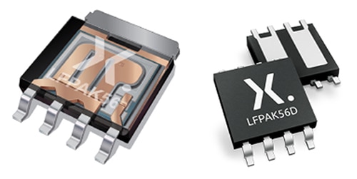 Figure 1: The LFPAK56D package (right) integrates two independent MOSFETs and uses copper clip structures similar to the LFPAK56 single MOSFET package (left). (Image source: Nexperia)
Like most parts intended for high-voltage switching converters, the LFPAK56D uses superjunction technology. This design reduces the drain-source “on” resistance (RDS(on)) and the gate-drain charge (QGD) parameters, minimizing power losses. Operating two MOSFETs on the same substrate further reduces drain-source resistance.
As superjunction MOSFETs, the LFPAK56D series is robust against avalanche events and has a wide safe operating area (SOA). For example, each of the 100 volt MOSFETs in the PSMN029-100HLX TrenchMOS device has a 29 milliohm (mΩ) RDS(on), can handle 68 watts, and can pass up to 30 amperes (A).
The LFPAK56D series also uses NXP's SchottkyPlus technology to reduce spiking behavior and leakage current. For example, the typical RDS(on) for the PSMN014-40HLDX is typically 11.4 mΩ, and the drain-source leakage current is an extremely low 10 nanoamperes (nA).
To fully utilize the high currents of MOSFETs, the PCB must be designed to dissipate high heat and ensure stable electrical connections. Multi-layer PCBs with sufficient vias and large, thick copper conductor tracks ensure high thermal performance.
Avoid thermal runaway
While fully switched-on power MOSFETs are thermally stable, thermal runaway is a risk when the drain current (ID) is low. In this operating state, localized heating tends to lower the threshold gate-source voltage (VGS(th)), meaning the device turns on more readily. This creates a positive feedback situation where the additional current causes more heating and an even lower VGS(th).
Figure 2 shows this effect for a constant drain-source voltage (VDS). As VGS increases, there is a critical ID known as the Zero Temperature Coefficient (ZTC). Above this current, there is negative feedback and thermal stability (blue zone); below it, the threshold voltage drop dominates, resulting in thermally unstable operating points that can lead to thermal runaway (red zone).
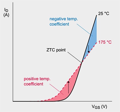 Figure 2: Below the ZTC point, the MOSFET can enter thermal runaway due to a thermally induced VGS drop (red area). (Image source: Nexperia)
This effect reduces the SOA at low currents and high drain-source voltages. This is not a significant concern for fast switching operations with a steep dV/dt slope. However, as the switching duration increases, e.g., to reduce electromagnetic interference, the thermal instability becomes more likely and potentially dangerous.
Lower switching losses at high frequencies
When selecting a superjunction MOSFET for fast switching applications, a low QGD is essential, as this significantly reduces switching losses.
High power loss occurs during switching when significant voltage and current changes appear simultaneously between the drain, gate, and source. A low QGD results in a short Miller Plateau (Figure 3, left), leading to a steep switching slope (dVds/dt) and ultimately resulting in lower dynamic energy loss during switch-on (Figure 3, blue area on the right).
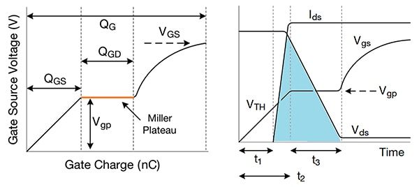 Figure 3: A short Miller Plateau (left) means a steep switching slope, resulting in low dynamic losses (blue area on the right). Vgp is the gate-source voltage of the Miller Plateau; VTH is the gate threshold voltage; IDS is the drain-source current. (Image source: Vishay)
Limiting avalanche energy and protecting the MOSFET
At the switch-off moment of a stator coil in a motor drive application, the collapsing magnetic field maintains the current flow, generating a high induction voltage across the MOSFET that superimposes upon the supply voltage (VDD). However, the reverse breakdown voltage (VBR) of the MOSFET body diode limits this high voltage. In what is known as the avalanche effect, the MOSFET converts the outflowing magnetic energy into avalanche energy (EDS) until the coil current drops to zero. This can quickly overheat the semiconductor crystal.
Figure 4 shows a simple coil control with a MOSFET switch and the time signals before, during (time window tAL), and after a single avalanche event. If the amount of avalanche energy dissipated (EDS(AL)S) is too high, the resulting heat will damage the semiconductor structure.
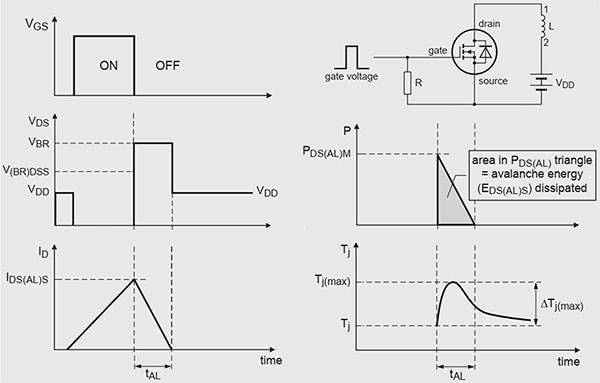 Figure 4: Timing signals of a MOSFET before, during (tAL), and after a single avalanche event. (Image source: Nexperia)
The LFPAK56D MOSFETs are designed to be very robust and can withstand several billion avalanche events without damage according to Nexperia’s laboratory tests. Considering the maximum avalanche energy, coil driver stages can dispense with additional freewheeling or clamping diodes and only use the avalanche operation of these MOSFETs.
Electro-thermal online simulation
To improve system efficiency, relying upon a simple Figure of Merit (FOM), such as the RDS x QGD product, is insufficient. Instead, designers need to carry out a more precise loss analysis that accounts for MOSFET losses resulting from:
- Switch-on conductivity
- Switch-on and switch-off losses
- Charging and discharging of the output capacitance
- Continuity and switching losses of the body diode
- Charging and discharging of the gate capacitance
To minimize overall losses, designers must understand the relationship between the MOSFET parameters and the operating environment. To this end, Nexperia offers precision electrothermal models for MOSFETs that combine electrical and thermal performance and represent all important MOSFET behaviors. Developers can use the PartQuest Explore online simulator or import the models in SPICE and VHDL-AMS format into their simulation platform of choice.
At the time of writing, only the electrical models are available for LFPAK56D MOSFETs. Therefore, the following thermal simulation example deals with a different MOSFET type, the BUK7S1R0-40H.
The interactive experiment IAN50012 Electrothermal models for Power MOSFET simulates three heating scenarios for the BUK7S1R0-40H MOSFET after a load current of 36.25 A is switched on. Figure 5 shows the three simulation setups on the left.
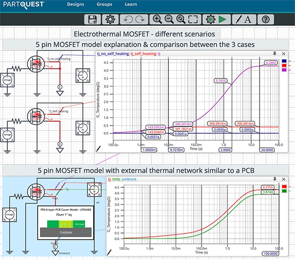 Figure 5: Shown is an electro-thermal simulation of a MOSFET using the PartQuest Explore online simulator. (Image source: Nexperia)
In the upper “tj_no_self_heating” case, the junction and mounting base are directly coupled to the ambient temperature (Tamb) of 0°C without thermal resistance (Rth). In the middle case, “tj_self_heating,” the chip is coupled via Rth-j, and Tj rises by around 0.4°C. The lower case shows a mounting base (mb) coupled to the ambient temperature via the Rth_mb of a six-layer FR4 board with a heatsink. Tmb (green) rises to 3.9°C and Tj (red) rises to 4.3°C.
Conclusion
Ultra-low-loss LFPAK56D MOSFETs provide excellent efficiency and power density in fast-switching converters or motor drivers. The circuit and thermal PCB design considerations and the electrothermal simulation discussed here illustrate how designers can overcome the challenges of robust, highly efficient, and space-constrained designs.
Disclaimer: The opinions, beliefs, and viewpoints expressed by the various authors and/or forum participants on this website do not necessarily reflect the opinions, beliefs, and viewpoints of DigiKey or official policies of DigiKey.


