Match Application Requirements More Effectively with Highly Integrated Arm® Cortex® MCUs
Contributed By DigiKey's North American Editors
2024-06-04
Developers face many challenges in meeting an expanding array of requirements for smart products in applications that include consumer, industrial, smart city, and healthcare. Each application brings its unique set of requirements concerning performance, security, ultra-low power consumption, long-range wireless connectivity, and cost. Too often, developers are forced to compromise with respect to those requirements due to a poor match between the application and the capabilities of available microcontroller unit (MCU) solutions.
This article introduces a set of processor solutions from STMicroelectronics that can deliver suitable performance combinations, battery life, security, and wireless connectivity that are critical for design success across a wide range of applications.
Meeting strict security requirements
STMicroelectronics’ STM32H7R/S bootflash MCUs (Figure 1) provide the high-performance, graphics, security, and reduced bill of materials (BOM) required in many smart products for industrial, consumer electronics, smart city, and healthcare applications. Based on a 600 megahertz (MHz) Arm® Cortex®-M7 processor with a double-precision floating-point unit (FPU), these MCUs feature integrated graphics, security subsystems, and a comprehensive set of peripherals and connectivity interfaces.
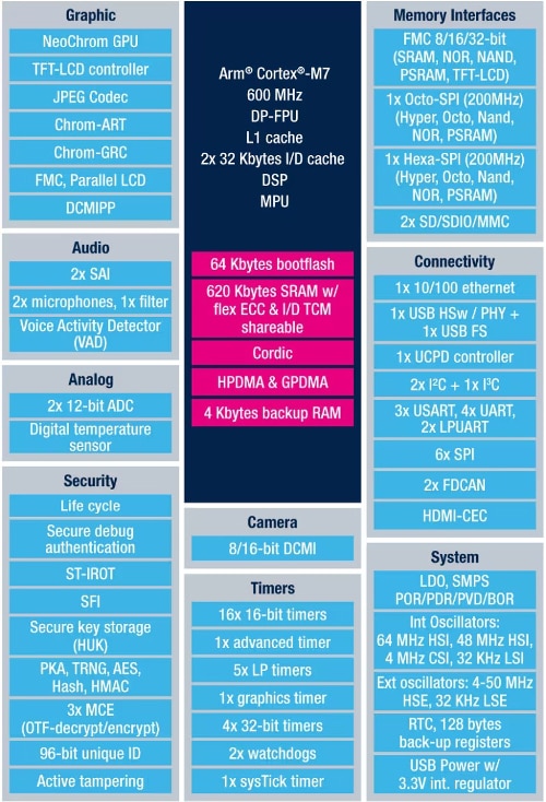 Figure 1: STM32H7R/S bootflash MCUs integrate a high-performance Arm Cortex-M7 with a full set of peripherals, functional blocks, and specialized capabilities needed to deliver secure smart products. (Image source: STMicroelectronics)
Besides the processors’ L1 cache comprising 32 kilobytes (KBytes) of instruction cache and 32 Kbytes of data cache, these MCUs come with 620 Kbytes of static random-access memory (SRAM), 64 Kbytes of embedded flash, and multiple interfaces for high-speed access to external memories. This combination of SRAM, embedded flash, and external memory access with execute-in-place (XiP) capability offers developers a high degree of flexibility when implementing high-performance and secure embedded systems.
To ensure security in applications running in external memory, STM32H7S MCUs also integrate three memory cipher engines (MCE) that perform on-the-fly encryption and decryption on external nonvolatile or volatile memories, with programmed access control to as many as four different regions for each MCE. Combined with additional hardware-based security features, including differential power analysis and protection against side-channel attacks, STM32H7S MCUs are certified to SESIP and PSA Assurance Level 3.
To ensure reliable performance of time-critical tasks such as interrupt service routines, some of the SRAM is mapped to the MCU’s tightly coupled memory (TCM) interface, providing zero-wait-state memory for critical instructions and data. To ensure system integrity, the MCU combines multiple security features with its embedded flash to enable secure boot and application integrity checking, providing a root of trust (RoT) for system and application software running in on-chip or off-chip memory. When combined with appropriate hardware-based protection mechanisms, this use of embedded flash for storing the trusted bootloader provides significant advantages in flexibility compared to the use of read-only memory (ROM) in traditional MCUs.
Multiple paths to secure boot
To provide the RoT essential for system security, secure boot relies on trusted immutable code that always runs immediately after system reset. This code verifies that only trusted software runs in the next phase of the system start-up sequence. With STM32H7R/S MCUs, developers have multiple paths to secure boot when building trusted systems. They can use prebuilt RoT firmware or control the boot sequence themselves (Figure 2).
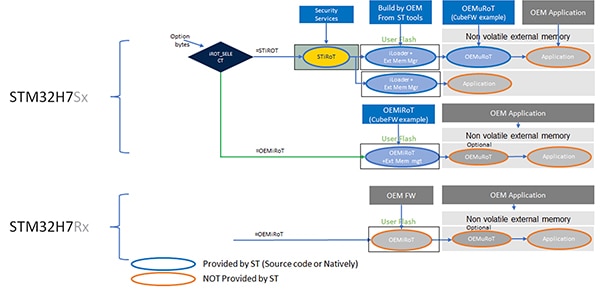 Figure 2: STM32H7R/S MCUs offer multiple boot paths designed to simplify development. (Image source: STMicroelectronics)
Following system reset, all STM32H7R/S MCUs begin the boot sequence by running the trusted root secure services (RSS) located in protected system flash memory. Subsequent steps in the boot sequence depend on the type of MCU and the developer’s choice of boot path. With each boot path, STM32H7R/S MCUs use their hide protection level (HDPL) mechanism to ensure temporal isolation of each boot level. As the boot sequence passes from one boot level to the next, the HDPL counter increments, and resources associated with the previous boot level are hidden from the current level.
Maintaining RoT through the entire boot sequence
In the boot path for STM32H7R-based production systems, RSS runs immediately on system reset. RSS runs the original equipment manufacturer’s (OEM) immutable RoT (iRoT) firmware located in the user flash memory. Because the HDPL is incremented at this next level, RSS remains hidden from the OEMiRoT firmware, which handles the next step in the boot sequence. If the application is designed to support updatable RoT (uRoT) firmware, the OEMiRoT runs the OEMuRoT firmware from external memory. In the final stage of the boot sequence, the OEMiRoT (or optional OEMuRoT) firmware runs the application code. The HDPL ensures that RSS, the OEMiRoT, and the optional OEMuRoT are all hidden from the application.
STM32H7S-based production systems can be configured to follow a boot path similar to that of STM32H7R systems, leaving complete control of the boot process to the developer. With STM32H7S MCUs, developers can also choose a highly secure path that invokes the prebuilt STMicroelectronics iRoT (STiRoT) firmware located in protected system flash memory.
In the STiRoT-enabled boot path, a routine (iLoader) located in protected embedded flash, loads code for the next boot level into internal SRAM. STiRoT then checks the integrity and authenticity of that code before allowing it to execute. For one-stage boot paths, iLoader loads the application code into SRAM. For two-stage boot paths, iLoader loads OEMuRoT from external flash into SRAM.
Once in internal SRAM, the application code (or OEMuRoT firmware) is checked for integrity and authenticity without the risk of an attack during the verification of code residing in external memory. Once validated, the OEMuRoT performs the integrity and authenticity checks on the application code before application execution. Developers can easily extend this two-stage boot path to validate updates to application code or even to the OEMuRoT firmware (Figure 3).
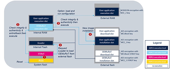 Figure 3: STM32H7S MCUs enable secure update and secure boot through a multistep process designed to ensure the integrity and authenticity of code at each step in the process. (Image source: STMicroelectronics)
During normal operation in production systems, the embedded flash in STM32H7R/S MCUs is in a closed state, where RoT firmware is provisioned and valid boot entry is enforced. These MCUs additionally provide a total of four PRODUCT_STATEs designed to support the entire product lifecycle (Figure 4).
|
Figure 4: STM32H7R/S MCUs operate in one of four PRODUCT_STATEs designed to support the entire product lifecycle. (Image source: STMicroelectronics)
Developers can control the PRODUCT_STATE in three ways:
- Non-volatile state (NVSTATE), which sets the flash memory in an open or closed state
- OEM provisioned (OEM_PROVD), which defines the stability of the secure hide protection (HDP) area that ensures that code executed in this area remains hidden after boot
- Debug authentication method (DBG_AUTH), which defines the method used to open the device debug
With these four states, STM32H7R/S MCUs support the security requirements of each critical phase of the product lifecycle: product development, product manufacturing, and field deployment (Figure 5).
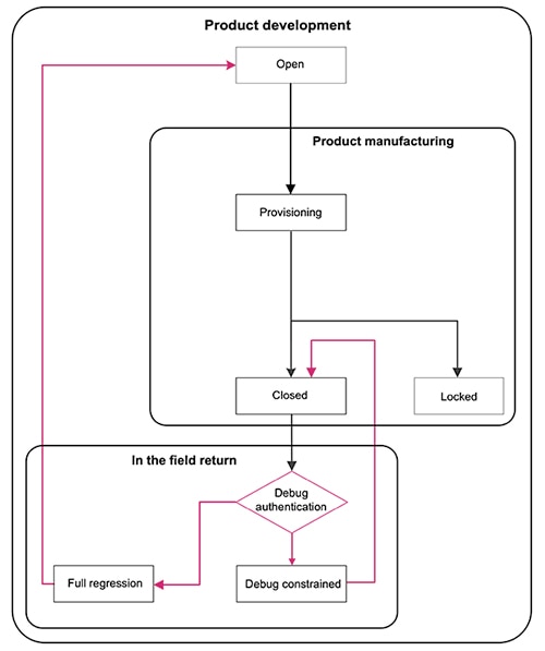 Figure 5: As a product moves from development and manufacturing to the field, STM32H7R/S MCUs can protect sensitive code and data in embedded flash while providing authenticated debug access when necessary. (Image source: STMicroelectronics)
In practice, debug authentication offers a powerful security feature designed to meet the practical challenges of product lifecycle support. For production systems operating in the closed state, developers can use an authentication protocol that allows a secure debugger to reopen access without compromising the RoT in a constrained debug session. In full regression debug, code and data security is not guaranteed.
Meeting the need for enhanced user interfaces in smart products
Although security remains paramount, smart products depend on increasingly sophisticated graphical user interfaces (GUIs). STM32H7R/S MCUs address this requirement using integrated graphics accelerators. These include the Chrom-ART accelerator in STM32H7R3/S3 MCUs and the NeoChrom graphics processing unit (GPU) in STM32H7R7/S7 MCUs. While the 2D Chrom-ART accelerator and 2.5D NeoChrom GPU support multiple formats with drawing and blitting operations, the NeoChrom GPU supports the operations required in texture mapping (Figure 6).
|
Figure 6: The Chrom-ART graphics accelerator in STM32H7R3/S3 MCUs and the NeoChrom GPU in STM32H7R7/S7 MCUs provide the graphics performance and functionality needed in GUIs for smart products. (Image source: STMicroelectronics)
For evaluation and development, STMicroelectronics offers its NUCLEO-H7S3L8 STM32 Nucleo-144 development board for the STM32H7R3 and the STM32H7S78-DK Discovery kit for the STM32H7S7.
Designed for rapid prototyping development, the Nucleo-144 board includes an integrated ST-LINK debugger/programmer and offers LEDs, pushbuttons, and multiple board connector options. The STM32H7S78-DK Discovery kit offers Wi-Fi, several LEDs and pushbuttons, an onboard STLINK-V3EC debugger/programmer, and multiple board connectors, including two for USB Type-C® and one Ethernet RJ45 connector.
For software development, STMicroelectronics provides its STM32Cube MCU package as part of its STM32Cube ecosystem. Along with hardware abstraction layer (HAL) modules, board support packages (BSPs), and low-layer register-level application programming interfaces (APIs), the STM32Cube MCU package offers middleware components, connectivity stacks, and sample code. For graphics development, the company offers the X-CUBE-TOUCHGFX graphical framework, which includes:
- The TouchGFX Designer tool for graphics application development and simulation
- The TouchGFX Engine hardware-accelerated graphics library
- The TouchGFX Generator, which is an STM32CubeMX plugin that lets developers configure and generate the TouchGFX abstraction layer used by the TouchGFX Engine to access the underlying hardware and operating system
Ensuring extended battery life
Minimum power consumption and maximum battery life remain key design drivers in many application areas. STMicroelectronics’ STM32U0 series MCUs are designed to deliver the energy savings and extended battery life required in many basic industrial, medical, smart-metering, and consumer applications. Built around an ultra-low-power 56 MHz Arm Cortex-M0+ processor, the STM32U0 MCU series features three different families to let developers choose the optimal configuration of SRAM, flash, and peripherals required for their designs.
The STM32U031 family offers the most compact configuration with 12 Kbytes of SRAM, up to 64 Kbytes of flash memory, multiple timers, analog peripherals, and connectivity options (Figure 7).
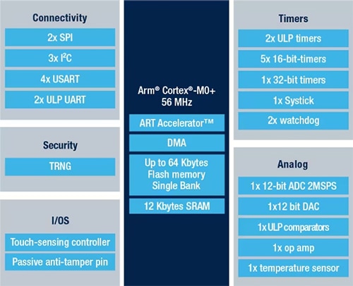 Figure 7: The three families in the STM32U0 MCU series build on an increasing set of features found in the STM32U031 MCU family. (Image source: STMicroelectronics)
Extending the features found in the STM32U031 family, the STM32U073 family adds an integrated LCD controller, additional connectivity channels, and analog peripherals, while offering 40 Kbytes of SRAM and up to 256 Kbytes of flash memory. The STM32U083 family builds upon those features by adding an Advanced Encryption Standard (AES) hardware accelerator.
Along with high integration, all STM32U0 series MCUs achieve ultra-low-power performance. In run mode, they consume only 52 microamps per megahertz (μA/MHz) while operating with their internal low-dropout (LDO) regulator.
Developers can choose from multiple low-power modes, including three stop modes, to minimize power consumption in battery-powered applications. For example, in the stop mode with the lowest power consumption, STM32U031 MCUs draw only 630 nanoamps (nA) with real-time clock (RTC) operation or 515 nA without it. In this same stop mode, STM32U073 and STM32U083 MCUs require only 825 nA with RTC or 695 nA without it. Nevertheless, all three families in the STM32U0 series running with a 24 MHz wake-up clock can reach run mode from this lowest power operating mode in only 12.0 microseconds (µs) in flash and 7.67 µs in SRAM.
Despite their ultra-low-power operation and thanks to their integrated adaptive real-time (ART) memory accelerator, these MCUs achieve performance equivalent to zero-wait-state execution from flash at a processor frequency of 56 MHz.
For development support, STMicroelectronics offers its NUCLEO-U031R8 STM32U031-based evaluation board, NUCLEO-U083RC STM32U083-based evaluation board, and STM32U083C-DK STM32U083-based Discovery kit. As with other devices in the STM32 family, the STM32Cube MCU package for the company’s STM32Cube ecosystem provides HAL modules, BSPs, low-layer APIs, middleware, connectivity stacks, and sample code.
Delivering long-range wireless connectivity
Efficient designs with long-range sub-gigahertz (GHz) wireless connectivity are essential in Internet of Things (IoT) applications for smart cities, agriculture, remote metering, remote sensing, and industrial systems. Many of these applications must maintain reliable communications despite interference from environmental sources such as the electrical power grid or machinery. This points to the use of interference-resistant long-range wide-area network (LoRaWAN) connectivity.
STMicroelectronics’ STM32WL5MOCH6TR module offers a LoRaWAN-certified solution capable of operating in Europe, Asia, and the Americas. This multiregional operating capability lies in the radio module’s support for 868 MHz European standards and 915 MHz North American standards supporting higher power output. The module’s support for multiple modulation schemes and its linear frequency range from 150 to 960 MHz enable it to support worldwide operation with various standard and proprietary communications protocols such as Sigfox, W-MBUS, and mioty.
Based on a dual-core architecture combining an Arm Cortex-M0+ and an Arm Cortex-M4, the STM32WL5MOC module combines its flexible radio transceiver, up to 64 Kbytes of SRAM, and up to 256 Kbytes of flash memory with a comprehensive security subsystem, timers, analog peripherals, connectivity interfaces, control features, and passive components for its embedded switch mode power supply (SMPS). In addition, the STMicroelectronics’ STSAFE-A100 secure element is included in the STM32WL5MOCH6STR variant (Figure 8).
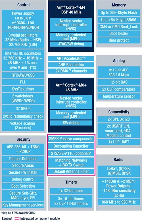 Figure 8: The STM32WL5MOC module provides a drop-in solution for sub-GHz connectivity, combining its dual-core architecture with a flexible radio, security features, multiple functional blocks, and passive components. (Image source: STMicroelectronics)
The STM32WL5MOC module’s extensive integrated functionality and LoRaWAN certification provide designers with an optimized drop-in hardware solution for long-range wireless applications. STMicroelectronics further speeds development with a comprehensive set of resources including the B-WL5M-SUBG1 expansion board, which combines an STM32WL5MOC module, 4 megabit (Mbit) flash memory, 256 kilobit (Kbit) EEPROM, STMicroelectronics microelectromechanical systems (MEMS) sensors, multiple board connectors, LEDs, and pushbuttons. For software development, the STM32CubeWL MCU package supports STM32WL series boards as part of the STM32Cube ecosystem.
Conclusion
Smart products for consumer, industrial, healthcare, and other applications have levels of security, power consumption, connectivity, and design complexity that rarely match the capabilities of a single microcontroller. The STM32 series of MCUs offers designers a broad choice of processing options to deliver an optimal match across diverse design requirements. Boards and software support the processors and simplify development.

Disclaimer: The opinions, beliefs, and viewpoints expressed by the various authors and/or forum participants on this website do not necessarily reflect the opinions, beliefs, and viewpoints of DigiKey or official policies of DigiKey.


