Leveraging Floating Ground Nonisolated Half-Bridge Gate Drivers
Contributed By DigiKey's North American Editors
2025-05-01
Product designers must balance multiple constraints—footprint, cost, reliability, and time-to-market. A key challenge is selecting a power supply that fits within the tight spaces required for modern applications.
Compact, high-performance power stages rely on fast, reliable gate drive solutions. These solutions vary from simple low-side drivers to fully isolated versions suited for high-voltage environments. For many designs, a floating ground nonisolated gate driver offers an efficient path to success.
Gate drivers act as intermediaries between low-power control signals—often from a microcontroller or pulse-width modulation (PWM) controller—and high-power switches that regulate energy flow. They ensure clean, rapid, and precise switching to optimize power delivery.
Selecting the right gate driver involves evaluating voltage and current requirements, topology, and switching frequency. A well-matched driver enhances efficiency, timing accuracy, and thermal stability—all critical for high-performance, compact systems.
Benefits of half-bridge topology
The half-bridge topology is a widely used approach in modern power conversion, enabling efficient voltage regulation in compact designs. It relies on two high-speed switching devices—typically MOSFETs or insulated-gate bipolar transistors (IGBTs)—that alternate the input voltage, either feeding a transformer in isolated designs or directly powering the load in nonisolated systems. This topology is valued for its efficiency and potential for thermal optimization.
A gate driver IC plays a crucial role in controlling these switches, acting as the interface between the controller and the power stage. It translates PWM signals into high-current drive signals, ensuring rapid and precise switching of the high-side and low-side transistors. This fast, efficient operation minimizes energy loss and enhances overall system performance.
In a half-bridge circuit, the high-side MOSFET’s source connects to the switching node, which rapidly moves between ground (0 V) and the input voltage (e.g., 12 V, 48 V, etc.) based on the switching cycle. With a floating ground nonisolated gate driver, the high-side driver “floats” with the voltage at the switching node, enabling clean and efficient transitions.
When isolation isn't required, and compactness, speed, and efficiency are priorities, floating ground nonisolated half-bridge gate drivers provide an ideal solution. Designed to control both high- and low-side MOSFET switches, these drivers eliminate the complexity of isolation while ensuring precise switching performance. Because they do not provide galvanic separation between the control logic and the power stage, they work best in systems where all components share a common ground.
Generating the required gate drive voltage for the high-side MOSFET typically relies on a bootstrap capacitor. This capacitor charges when the low-side switch is active and supplies power when the high-side switch turns on.
When the low-side MOSFET conducts, the switching node is pulled to ground, allowing a small diode-capacitor circuit to charge the bootstrap capacitor from the supply rail. When the high-side MOSFET needs to turn on, the driver taps into this stored charge to drive the gate to a voltage higher than the switching node—often 10 V to 15 V greater.
Designers must ensure the low-side switch turns on frequently enough to recharge the bootstrap capacitor. In high-duty-cycle applications, additional precautions may be necessary, such as selecting the right capacitor value and minimizing voltage drop across the bootstrap diode.
By leveraging bootstrap architecture and tracking the switching node voltage, floating ground nonisolated half-bridge drivers eliminate isolation complexity while ensuring robust high-side control. Their simplicity and efficiency make them well-suited for high-frequency switching applications like buck and boost converters, synchronous regulators, motor drives, and class-D audio amplifiers.
Selecting the right gate driver IC
Selecting the right gate driver is essential for ensuring efficient, reliable, and safe operation of the power stage, particularly in high-speed switching applications like buck converters, motor drives, and solar power systems. While gate drive fundamentals apply broadly, certain selection criteria become especially critical depending on system requirements.
In solar power conversion and battery-fed systems, for instance, the gate driver must accommodate wide input voltage variations and shifting load conditions. A high-side voltage rating with sufficient headroom is necessary to withstand full supply rail fluctuations and ensure long-term reliability.
Common-mode transient immunity (CMTI) is another key consideration. Fast switching events can generate steep voltage differentials between high-side and low-side MOSFETs, leading to noise and ringing. Gate drivers with high CMTI provide better stability in electrically noisy environments.
Peak drive current is equally important, particularly in high-power applications. The driver must supply enough current to quickly charge the MOSFET gate and overcome parasitic capacitance, reducing switching losses and improving thermal performance.
Finally, dead time control plays a crucial role in half-bridge configurations. Without a brief delay between turning off one switch and activating the other, shoot-through can occur—where both MOSFETs conduct simultaneously. Many gate drivers incorporate built-in or adjustable dead time settings to prevent this issue and enable safe, efficient operation across varying load conditions.
ADI's LTC706x family
The simplicity and high-speed switching capabilities of floating ground nonisolated half-bridge drivers make them an optimal solution for many designs. Analog Devices, Inc. (ADI) offers a range of feature-rich, high-voltage devices engineered for demanding applications.
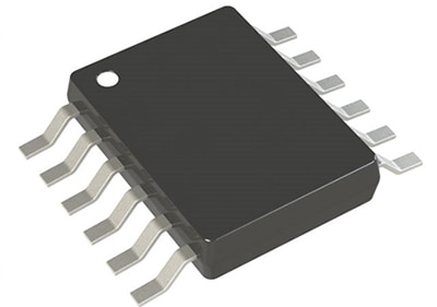
ADI's LTC706x floating ground nonisolated half-bridge gate drivers (Figure 1) offer versatile solutions to meet the demands of high-speed, high-voltage power conversion. Catering to a wide array of applications from automotive to industrial control, these devices provide tight timing control, shoot-through protection, and strong drive strength in compact packages.
 Figure 1: The form factor of ADI's LTC706x floating ground nonisolated half-bridge drivers. (Image source: Analog Devices, Inc.)
Providing a range of options to match voltage, logic, and layout requirements, the ADI products help designers achieve the right balance between system-level performance and simplicity. All support N-channel MOSFETs to provide lower on-resistance (RDSON), faster switching speeds, and higher current-handling capabilities than P-channel MOSFETs.
Two devices support a 100 V maximum supply voltage:
- The LTC7060 is optimized for systems that rely on a single PWM input with tri-state capability, allowing it to derive both high and low-side gate drive timing from one control line. This simplifies digital controller interfaces and reduces pin count for use in space-constrained applications. The tri-state input mode also enables a safe high-impedance state, adding a layer of fault tolerance in certain failure scenarios. It's a good choice for designers favoring simplicity and compactness.
- The LTC7061 is designed for applications that provide independent CMOS or TTL logic-level inputs for the high-side and low-side switches. This dual-input approach allows for greater flexibility and control over timing—especially valuable in systems where dead time is managed externally by a microcontroller or PWM controller. For designers needing tight control over switching behavior or implementing custom timing strategies, the LTC7061 offers a more adaptable interface with control flexibility to dial in performance.
For applications where input voltages exceed 100 V—such as industrial motor drives, automotive 48 V rails, or power-over-Ethernet infrastructure—designers can take advantage of two options supporting a 140 V maximum supply voltage:
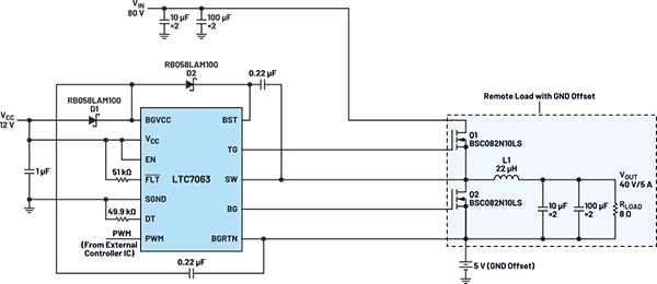
- The LTC7063 features a three-state PWM input, allowing control of both high-side and low-side MOSFETs through a single input signal. This configuration simplifies the control interface, as the PWM pin determines the state of the MOSFETs based on its voltage level. Designers may favor this for high-power applications that benefit from a simplified control interface, reduced pin count, and minimized signal routing complexity on dense PCBs. One practical application of the LTC7063 is in a 2:1 step-down converter design with a remote load (Figure 2). Operating from an input supply up to 80 V, this configuration delivers half of the input voltage (½ VIN) to a maximum load of 5 A.
 Figure 2: A step-down converter design with remote load using the LTC7063 floating ground nonisolated half-bridge gate driver. (Image source: Analog Devices, Inc.)
- The LTC7066 accepts independent CMOS/TTL logic-level inputs for the high-side and low-side drivers, providing separate control signals for each MOSFET. This allows for precise and flexible control, letting designers take full advantage over timing, dead-time, and switching behavior. This makes it ideal for systems with fine-tuned digital control, such as those using high-performance digital controllers or FPGAs.
Whether operating in low or high-voltage environments, each device in the lineup includes essential protections and tuning parameters that help designers extract maximum performance from the power stages.
Each product provides adaptive shoot-through protection to prevent both high-side and low-side MOSFETs from conducting at the same time. In addition, each device supports adjustable dead-time, allowing designers to fine-tune the delay between switching transitions to minimize losses and avoid cross-conduction without sacrificing efficiency. Undervoltage lockout (UVLO) is another common feature, ensuring that the gate driver only operates when supply voltages are within safe thresholds.
From a performance perspective, LTC706x devices all offer strong gate drive impedance, with typical values of 1.5 Ω pull-up and 0.8 Ω pull-down. This enables rapid gate charging and discharging—critical for fast switching, tight timing control, and reduced switching losses in high-speed applications.
For high-duty-cycle applications where conventional bootstrap methods are inadequate, designers can evaluate alternative gate drive techniques. The trade-offs of each in terms of complexity, efficiency, and cost will have to be considered. Isolated gate drivers, for example, utilize transformers or digital isolators to deliver independent gate drive voltages, thereby eliminating the need for bootstrap charging mechanisms, while direct bias supplies can provide a stable gate drive voltage independent of switching cycles.
Conclusion
In high-power applications where speed, efficiency, and compact design are paramount, floating ground nonisolated half-bridge gate drivers provide an optimal solution for controlling both high-side and low-side MOSFETs. By leveraging a bootstrap circuit to generate the necessary gate drive voltage, these drivers eliminate the complexity of isolated designs while maintaining precise switching performance. ADI's LTC706x product family provides a range of versatile solutions to meet the demands of high-speed, high-voltage power conversion.

Disclaimer: The opinions, beliefs, and viewpoints expressed by the various authors and/or forum participants on this website do not necessarily reflect the opinions, beliefs, and viewpoints of DigiKey or official policies of DigiKey.


