How to Use Zero-Drift Op-amps to Achieve Precise, Accurate, Low-Power Industrial System Control
Contributed By DigiKey's North American Editors
2020-10-22
As industrial systems move increasingly from mechanical to electronic control, manufacturers are seeing gains in both product quality and worker safety; the latter being mainly due to workers being more protected from harsh environments. However, it is those harsh environments, with temperature extremes as well as electrical noise and electromagnetic interference (EMI), that make good signal conditioning so critical to maintaining both the circuit stability and sensitivity required for reliable, precise and accurate control over industrial machinery’s operating lifetime.
A critical component in the signal conditioning chain is the operational amplifier (op-amp), a high-gain DC differential amplifier used to acquire and amplify required signals. Standard op-amps are susceptible to temperature drift and have limited precision and accuracy; so, to meet industrial requirements, designers add some form of system-level automatic calibration. The problem is that this calibration function can be complex to implement and increases power consumption. It also requires more board space and adds to cost and design time.
This article will review the signal conditioning requirements of industrial applications and what designers need to be concerned about. It will then introduce high-performance zero-drift op-amp solutions from ON Semiconductor and show why and how they can be used to meet industrial signal conditioning requirements. Other relevant characteristics of these devices such as high common mode rejection ratios (CMRRs), high power supply rejection ratios (PSRRs), and high open-loop gain will also be examined.
Industrial signal-conditioning applications
Low-side current sensing and sensor interfaces are often used in industrial systems. Due to the very small differential signals associated with these circuits, designers need high-accuracy op-amps.
Low-side current sensing is used to detect over-current conditions and is often used in feedback control (Figure 1). A low value sense resistor (<100 milliohms (mΩ)) is placed in series with the load to ground. The low value of the resistor reduces power losses and heat generation but results in a correspondingly small voltage drop. A precision zero-drift op-amp can be used to amplify the voltage drop across the sense resistor with a gain set by external resistors R1, R2, R3, and R4 (where R1 = R2, R3 = R4). Precision resistors are required for high accuracy, and the gain is set to utilize the full scale of the analog-to-digital converter (ADC) for the highest resolution.
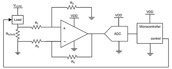 Figure 1: Low-side current sensing showing the op-amp interface between the sense resistor and the ADC. (Image source: ON Semiconductor)
Sensors used to measure strain, pressure and temperature in industrial and instrumentation systems are often configured in a Wheatstone bridge configuration (Figure 2). The sensor voltage change that provides the measurement can be quite small and has to be amplified before going into the ADC. Precision zero-drift op-amps are often used in these applications due to their high gains, low noise and low offset voltages.
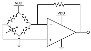 Figure 2: Precision op-amps are often used with Wheatstone bridges to amplify the signal from sensors for strain, pressure, and temperature before sending that signal to an ADC. (Image source: ON Semiconductor)
Key parameters for precision op-amps
Offset voltage, offset voltage drift, susceptibility to noise and open-loop voltage gain are the key parameters that limit op-amp performance in current sensing and sensor interface applications (Table 1).
 Table 1: Key parameters for precision op-amps that affect accuracy and precision. (Image source: ON Semiconductor)
Input offset voltage (denoted by VOS or VIO, depending on the manufacturer) derives from imperfections in the semiconductor manufacturing process that cause a differential voltage between VIN+ and VIN-. It is a part-to-part variation that can drift over temperature and can be positive or negative making it difficult to calibrate out. Designers’ efforts to reduce the offset or drift in standard op-amps not only adds complexity, but in some cases can result in increased power consumption.
For example, consider current sensing using an op-amp in a difference amplifier configuration (Figure 3).
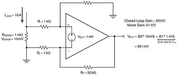 Figure 3: Current sensing with an op-amp in a difference amplifier configuration. Low offset voltage is critical since the input offset voltage is amplified by the noise gain, creating an offset error at the output (noted as “Error due to VOS”). (Image source: ON Semiconductor)
The output voltage is the sum of the signal gain term (VSENSE) and the noise gain term (VOS), as shown in Equation 1:
![VOUT = (VSENSE x RF/R1) + (VOS x [1 + RF/R1]) Equation 1](http://sc-a.digikeyassets.com/-/media/Images/Article%20Library/TechZone%20Articles/2020/October/How%20to%20Use%20Zero-Drift%20Op%20Amps%20to%20Achieve%20Industrial%20System%20Control/article-2002october-how-touse-zero-drift-equation1.jpg?la=en&ts=41c863e8-cf99-46af-9354-34a51ce4a00a) Equation 1
Equation 1
As an internal op-amp parameter, the input offset voltage is multiplied by the noise gain and not the signal gain, resulting in an output offset error (“Error due to VOS” in Figure 2). Precision op-amps minimize the offset voltage as much as possible using various techniques. In zero-drift op-amps, this applies particularly to low frequency and DC signals. The offset voltage of precision zero-drift op-amps can be over two orders of magnitude lower compared to general purpose op-amps (Table 2).
 Table 2: In a comparison of the maximum offset voltage of selected general-purpose op-amps and chopper-stabilized zero-drift op-amps, the offset voltage of precision zero-drift op-amps can be over two orders of magnitude lower. (Image source: ON Semiconductor)
Zero-drift op-amps
With their improved performance, designers can meet the signal conditioning requirements of industrial applications using zero-drift op-amps. Two examples of zero-drift op-amps that offer different levels of performance are ON Semiconductor’s NCS325SN2T1G and the NCS333ASN2T1G. Designers can use the NCS325SN2T1G device for precision applications that can benefit from a 50 microvolt (µV) offset and a drift of 0.25 µV/°C, while the NCS333ASN2T1G family is suited for the most demanding high-precision applications, delivering a 10 µV offset and a drift of only 0.07 µV/°C. These two op-amps achieve zero drift using different internal architectures.
The NCS333ASN2T1G uses a chopper-stabilized architecture, which provides the advantage of minimizing offset voltage drift over temperature and time (Figure 4). Unlike the classical chopper architecture, the chopper-stabilized architecture has two signal paths.
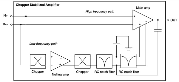 Figure 4: The NCS333ASN2T1G has two signal paths: the second path (bottom) samples the input offset voltage, which is used to correct the offset at the output. (Image source: ON Semiconductor)
In Figure 4, the lower signal path is where the chopper samples the input offset voltage, which is then used to correct the offset at the output. The offset correction occurs at a frequency of 125 kilohertz (kHz). The chopper-stabilized architecture is optimized for best performance at frequencies up to the related Nyquist frequency (1/2 of the offset correction frequency). As the signal frequency exceeds the Nyquist frequency, 62.5 kHz, aliasing may occur at the output. This is an inherent limitation of all chopper and chopper-stabilized architectures.
Nevertheless, the NCS333ASN2T1G op-amp has minimal aliasing up to 125 kHz and low aliasing up to 190 kHz. ON Semiconductor’s patented approach utilizes two cascaded, symmetrical, resistor-capacitor (RC) notch filters tuned to the chopper frequency and its fifth harmonic to reduce aliasing effects.
Auto-zero architecture
Another approach to zero-drift op-amps is the auto-zero architecture (Figure 5). The auto-zero design has a main amp and a nulling amp. It also uses a clocked system. In the first phase, the switched capacitors hold the offset error from the previous phase on the nulling amp output. In the second phase, the offset from the nulling amp output is used to correct the offset of the main amp. The NCS325SN2T1G from ON Semiconductor is built using the auto-zero architecture.
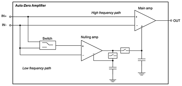 Figure 5: Simplified block diagram of an auto-zero op-amp like the NCS325SN2T1G showing the switched capacitors. (Image source: ON Semiconductor)
In addition to the differences between the NCS333ASN2T1G (chopper-stabilized architecture) and NCS325SN2T1G (auto-zero architecture) in terms of offset voltage and drift described above, the different architectures produce differences in open-loop voltage gain, noise performance and aliasing susceptibility. The NCS333ASN2T1G has an open-loop voltage gain of 145 decibels (dB), while the NCS325SN2T1G has a 114 dB open-loop voltage gain. Considering noise, the NCS333ASN2T1G has a CMRR of 111 dB and a PSRR of 130 dB, while the NCS325SN2T1G has a CMRR of 108 dB and a PSRR of 107 dB. Both have very good ratings, but the NCS333ASN2T1G outperforms the NCS325SN2T1G.
The NCS333ASN2T1G series op-amps also have minimal aliasing. This is because of ON Semiconductor’s patented approach using two cascaded, symmetrical, RC notch filters tuned to the chopper frequency and its fifth harmonic to reduce aliasing effects. In theory, an auto−zero architecture will exhibit more dramatic aliasing than a chopper-stabilized type. But aliasing effects can vary widely and are not always specified. It is up to the designer to understand the aliasing characteristics of the specific op-amp being used. Aliasing is not a defect of sampling amplifiers, it is a behavior. Knowledge of this behavior and how to avoid it can make zero−drift amplifiers operate at their best.
Finally, op-amps have varying amounts of EMI susceptibility. Semiconductor junctions can pick up and rectify EMI signals, creating an EMI−induced voltage offset at the output, adding another component to the total error. Input pins are the most sensitive to EMI. The high precision NCS333ASN2T1G op-amp integrates low-pass filters to decrease sensitivity to EMI.
Design and layout considerations
To ensure optimum op-amp performance, it is mandatory that designers follow good pc board design practices. High precision op-amps are sensitive devices. For example, placing 0.1 microfarad (µF) decoupling capacitors as close as possible to the supply pins is important. Also, when making a shunt connection, the circuit board traces should be of equal length, equal dimension and as short as possible. The op-amp and the shunt resistor should be on the same side of the board, and for applications that require the highest level of accuracy, four-terminal shunts, also called Kelvin shunts, should be used. These combined techniques will reduce EMI susceptibility.
Always follow the shunt manufacturer’s recommendations on connecting to it. An improper connection will add unwanted stray lead and sense resistance to the measurement and increase error (Figure 6).
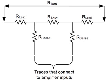 Figure 6: Connection to a two-terminal shunt resistor depicting stray resistances (RLead and RSense). (Image source: ON Semiconductor)
The accuracy can be affected by temperature-dependent offset voltage variations at the input pins. To minimize these variations, designers should use metals with low thermoelectric coefficients, and prevent temperature gradients from heat sources or cooling fans.
Conclusion
The need for precise and accurate signal conditioning is growing across a range of industrial applications. Accompanying this growth is the need for low-power, compact solutions. Op-amps are critical components in signal conditioning, but designers have needed to add auto-calibration and other mechanisms to ensure stability across time and temperature, adding complexity, cost, and additional power consumption.
Fortunately, designers can turn to high-performance zero-drift op-amps with continuous auto-calibration, very low offset voltages, and near zero drift over time and temperature. In addition, they have low power consumption over a wide dynamic range, are compact, and feature high CMRRs, high PSRRs, and high open-loop gain, all key characteristics for industrial applications.
Recommended Reading

Disclaimer: The opinions, beliefs, and viewpoints expressed by the various authors and/or forum participants on this website do not necessarily reflect the opinions, beliefs, and viewpoints of DigiKey or official policies of DigiKey.


