How to Use SSRs for Reliable, Fast-Switching, Low-Loss Semiconductor Automated Test Equipment
Contributed By DigiKey's European Editors
2024-01-18
Integrated circuits (ICs) are more in demand than ever because they reduce hardware development costs, promote the miniaturization of electronic devices, and provide a wide range of functions. To ensure the quality of large production batches, semiconductor manufacturers require reliable and compact automated test equipment (ATE) that can quickly switch high-frequency AC and DC currents with low and high signal levels and minimal loss.
Solid-state relays (SSRs) based on photovoltaic MOSFETs are ideal for IC testers and ATE applications. Their miniature size and wear-free properties are particularly interesting.
This article briefly discusses ATE requirements. It then introduces different types of photovoltaic MOSFET relays from Panasonic's PhotoMOS series SSRs and highlights their differences in component geometry and switching characteristics. Design tips for accelerated on/off switching and reducing PhotoMOS-specific leakage currents conclude the topic.
High packing density and short signal paths
An automated IC tester makes contact with the device under test (DUT) using densely packed needle adapters (probe cards) to perform functional testing. The modules in the test head generate and distribute high-speed test pulses, supply appropriate voltages, and switch measurement channels. Every test must occur in a confined space to minimize line losses, signal propagation times, interference, and channel crosstalk.
For this task, designers can use small-format switching elements such as Panasonic’s AQ series relays. For example, the voltage-controlled CC type AQY2C1R6PX PhotoMOS SSR comes in a TSON package that occupies 3.51 square millimeters (mm2) (1.95 × 1.80 mm) (Figure 1). It uses capacitive coupling to provide 200 volt isolation protection and is voltage controlled, requiring only 1.2 milliwatts (mW) of control power.
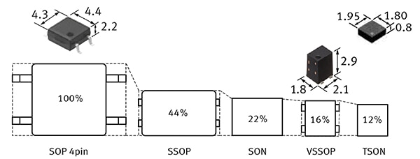 Figure 1: Shown are the housing dimensions for the AQ series small-signal PhotoMOS relays; dimensions are in millimeters. (Image source: Panasonic, modified by author)
The current-controlled RF type AQY221R6TW PhotoMOS relay has a small footprint of 3.8 mm², but its VSSOP housing is 3.6 times taller than the AQY2C1R6PX. It requires only 75 mW of control power and uses optical coupling to provide 200 volts of protective isolation. The leakage current (ILeak) of the CC and RF types is very low at 10 nanoamperes (nA).
Figure 2 shows the circuit principle of CC type relays with capacitive coupling (left), and the RF type with optical coupling (right).
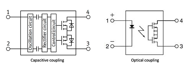 Figure 2: The AQY2C1R6PX CC type PhotoMOS SSR (left) uses capacitive coupling and is voltage driven; the AQY221R6TW RF type (right) uses optical coupling and is current driven. (Image source: Panasonic, modified by author)
The GE type AQV214EHAX also uses optical coupling and offers significantly higher protective insulation of up to 5 kilovolts (kV) between the control circuit (IN) and the load circuit (OUT). It comes in a larger 6-SMD package that measures 8.8 mm x 6.4 mm with gull-wing leads. Requiring only 75 mW control power, SSRs from the GE series switch load currents of up to 150 mA at a maximum of 400 volts.
Optimizing contact resistance and output capacitance
As is typical for semiconductors, SSRs have an “on” resistance (Ron) and output capacitance (Cout) that cause heat loss and leakage current, respectively. Different relay types optimize for one or the other depending on the kind of signal to be switched.
SSR types with a particularly low Ron cause less attenuation when switching high-frequency AC test pulses. SSRs with a low Cout enable more accurate measurements for DC signals, while types with a high Cout are suitable for switching higher power levels. Figure 3 shows an automated semiconductor test system and illustrates which PhotoMOS relay types are best suited to various signal paths in the measuring module of the test head.
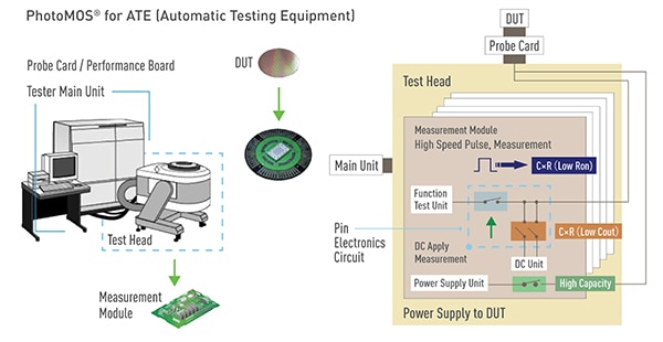 Figure 3: Each signal path of this automated semiconductor test system requires a specific PhotoMOS relay type. (Image source: Panasonic)
The AQY2C1R3PZ and AQY221N2TY PhotoMOS relays feature a low Cout of 1.2 and 1.1 picofarads (pF), respectively. This allows them to switch on and off at up to 10 and 20 microseconds (µs) (AQY2C1R3PZ), and 10 and 30 µs (AQY221N2TY). The tradeoff for both relays is increased Ron, 10.5 and 9.5 Ω, respectively, resulting in higher losses and component heating. These PhotoMOS relays are good for quickly switching measurement signals with low current flow, and they generate less reflection/phase shift with high-frequency signals.
The AQY2C1R6PX and AQY221R6TW discussed earlier are more suitable for slower-switching power signals and supply voltages with higher currents. While their lower Ron causes less component heating, their larger Cout has an integrator effect on the signals.
Minimizing signal distortion
Semiconductor relays that only represent a simple on/off switch (1 form A) are examples of phototriacs for AC signals or optocouplers with bipolar transistors for pulsating DC signals. These devices cause distortions in the load signal due to threshold, ignition voltages, and switching delays. In addition, reverse recovery currents can generate harmonic overshoots (ringing) and leakage currents of several 10 to 100 milliamperes (mA).
The FET half-bridge with driver circuit in Panasonic's PhotoMOS relays minimizes these signal distortions, hence their suitability for low-loss switching of AC and DC small signals such as high-speed test pulses, measurement signals, and supply voltages. When switched off, the leakage currents between the two OUT connections are below 1 microampere (µA).
PhotoMOS relays are available in form A (single pole, single throw, normally open contact (SPST-NO)) or form B (normally closed contact, SPST-NC), and as multiples. Designers can build form C switches such as single pole, double throw (SPDT); single-pole changeover switches; and double pole, double throw (DPDT) switches by combining form A and form B devices.
For example, the AQS225R2S is a quadruple PhotoMOS relay (4SPST-NO) in a SOP16 housing that can handle a maximum of 70 mA at switching voltages up to 80 volts. Also, the AQW214SX is a dual PhotoMOS relay (2SPST-NO) in a SOP8 housing that can handle load currents up to 80 mA at switching voltages up to 400 volts.
Figure 4 shows the internal structure of an SSR, PhotoMOS, and a photocoupler, along with their typical signal distortions. PhotoMOS relays do not cause signal clipping or similar distortions on ohmic loads.
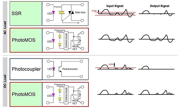 Figure 4: SSRs and photocouplers cause distortions in the output signal due to threshold and ignition voltages; PhotoMOS relays switch AC and DC signals without distortion. (Image source: Panasonic, modified by author)
To attenuate the feedback effect of inductive and capacitive switching loads, thus protecting the PhotoMOS output stage, designers must add clamp and freewheeling diodes, RC and LC filters, or varistors on the output side. In the CC series, clamp diodes protect the input oscillator from overvoltage peaks and limit the control signal to 3 volts to 5.5 volts, while RC filters ensure a residual ripple of less than ±0.5 volts.
Reducing leakage currents
The Cout of PhotoMOS relays serves as a bypass for alternating currents and pulse sequences of higher frequency when the relay is de-energized. To significantly reduce such leakage currents and maximize isolation at high frequencies, Panasonic recommends using three separate PhotoMOS relays in the form of a T-circuit (Figure 5, left). In the main signal path, the two 1 Form A PhotoMOS relays, S1 and S2, are low-Ron types, while a low-Cout type forms the 1 Form A short-circuit switch, S3.
 Figure 5: When S1 and S2 are de-energized, the switched-on relay S3 acts as a short circuit for all leakage currents (T-circuit OFF state, right). (Image source: Panasonic, modified by author)
T-circuit ON state (Figure 5, center): In the case of S1 and S2 switched on, their Ron minimally attenuates the signal level, while the low Cout from the switched-off S3 relay slightly attenuates high frequencies (low pass).
T-circuit OFF state (Figure 5, right): If S1 and S2 are de-energized, their Cout represents a bypass for high frequencies (high pass), but the switched-on S3 relay short circuits the signals capacitively passed through S1 (suction circuit).
The ON/OFF timing of the T-circuit must be implemented as a break before make (BBM) switch. Accordingly, S1 and S2 should be deactivated before S3 is turned on. With relays, BBM means that the contacts switch over separately, whereas make before break (MBB) means they switch over in a bridging manner.
Switching PhotoMOS relays faster
The internal photosensor of the PhotoMOS relay works as a solar cell and supplies the gate charging current. As such, a brighter light pulse from the LED increases the switching speed. For example, the bootstrap element R1/R2/C1 in Figure 6 generates a higher current pulse.
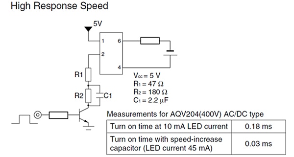 Figure 6: The bootstrap element R1/R2/C1 increases the switch-on speed of the PhotoMOS relay. (Image source: Panasonic)
C1 acts as a short circuit for R2 at the moment of switch-on, so the low resistance of R1 allows a high current to flow. If C1 is charged and has a high resistance, R2 is added, reducing the flow to the holding current, as with magnetic relays. The AQV204 PhotoMOS relay thus reduces its switch-on time from 180 µs to 30 µs.
Conclusion
By using small, wear-free PhotoMOS relays, designers can improve ATE applications' signal density and measurement speed while reducing maintenance needs. Additionally, following recommended design techniques can help minimize leakage currents and switching times.

Disclaimer: The opinions, beliefs, and viewpoints expressed by the various authors and/or forum participants on this website do not necessarily reflect the opinions, beliefs, and viewpoints of DigiKey or official policies of DigiKey.


