How to Use FPGAs in Resource-Constrained Applications
Contributed By DigiKey's North American Editors
2025-05-07
The need for configurable logic is growing across resource-constrained embedded systems. Applications such as edge AI, machine vision, and industrial automation require flexible, application-specific logic to meet evolving performance demands while operating within strict power, size, and cost limits. Modern field programmable gate arrays (FPGAs) can address these competing demands.
This article reviews key design criteria to consider when selecting an FPGA for resource-constrained applications. It then describes how different product lines align with specific scenarios using examples from Altera’s portfolio of power and cost-optimized FPGAs. It concludes by highlighting development kits and evaluation boards that can be used to prototype and validate design concepts.
Considerations for choosing an FPGA
Choosing an FPGA for a resource-constrained system involves consideration of multiple design requirements and matching those to the correct solution. There are several key FPGA characteristics to consider:
Logic element (LE) capacity: As the fundamental building block for an FPGA, the number of LEs determines how much custom logic can be implemented. Higher counts enable more complex designs: the tradeoff is increased power, cost, and package size.
I/O and memory: FPGAs are often used to connect disparate components within a system, making the number of I/O pins a key consideration. To boost I/O performance, many FPGAs incorporate hardened, fixed-logic blocks for interfaces such as PCI Express (PCIe), high-speed memory, and multi-gigabit transceivers.
In addition, some FPGAs integrate features such as analog-to-digital converters (ADCs) and Flash memory. These enhancements can reduce the need for companion chips, conserving board space and improving power efficiency.
Processor integration: Instead of using an external processor, a “soft” microprocessor unit (MPU) can be implemented within the FPGA. This approach can reduce the footprint of a system, but it is best suited to applications with less demanding MPU workloads.
For applications that need faster, more efficient MPUs, designers can consider an FPGA with a hard processor system (HPS) that will implement an MPU as a fixed-logic block within the FPGA.
Hardware accelerators: FPGAs typically include dedicated digital signal processing (DSP) blocks that efficiently handle compute-intensive tasks like motion control. Higher-end devices may feature specialized tensor blocks for AI workloads. The capabilities of these accelerator blocks vary significantly between FPGA families and can dramatically influence overall system performance.
Package and power optimizations: Some FPGAs are specifically designed to minimize their physical and electrical footprint. For example, they may offer low-power sleep modes.
Tools: Crafting custom logic can be a daunting challenge, particularly for designers who are new to the process. Tools like Altera’s Quartus Prime Design Software have emerged to streamline the process.
Built to make FPGA design more accessible, Quartus Prime offers a developer-friendly experience, an extensive catalog of pre-built logic blocks, and the ability to interconnect these logic blocks automatically. The tool integrates with popular AI and machine learning (ML) workflows, enabling developers to deploy popular operating systems (OSs) like Linux and Zephyr on an FPGA.
Capabilities like these can significantly accelerate FPGA design, making tool features a critical consideration when selecting a device.
High-performance compute for advanced embedded workloads
To illustrate how design requirements influence FPGA selection, it is helpful to begin with high-end applications that require exceptional compute density, bandwidth, and integration. Examples include advanced edge AI applications and high-performance industrial gateways.
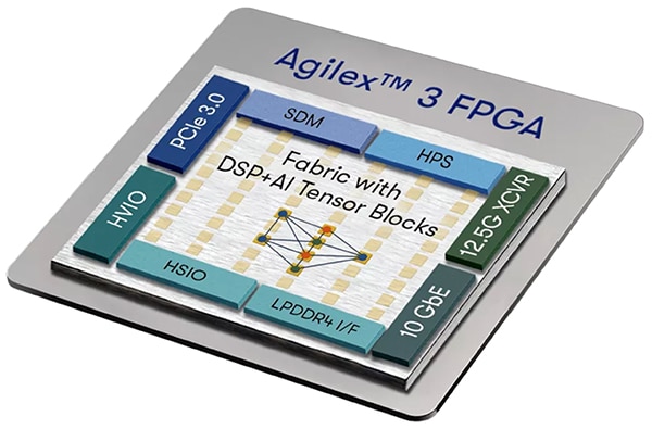
Agilex 3 FPGAs (Figure 1) are designed to meet these application demands, offering up to 135K LEs. The chips are available in both FPGA-only and system-on-chip (SoC) variants. The SoC devices integrate a dual-core, 800 megahertz (MHz) Arm® Cortex®-A55, enabling the FPGA to take on complex software stacks like human-machine interfaces (HMIs) or network stacks.
The programmable fabric features AI Tensor blocks capable of delivering up to 2.8 INT8 tera operations per second (TOPS). These blocks support various compute formats, including FP16, FP19, FP32, and BFLOAT16, and are optimized for efficient execution of AI workloads. Variable-precision DSP blocks are also included, delivering up to 180 giga floating-point operations per second (GFLOPS) performance for general-purpose signal processing.
 Figure 1: The Agilex 3 is notable for its high-performance DSP and AI Tensor blocks. (Image source: Altera)
High-speed connectivity is another strength of the Agilex 3 architecture. Transceivers support data rates up to 12.5 gigabits per second (Gbits/s), with hardened I/O blocks available for PCIe 3.0, 10 gigabit Ethernet (GbE), and LPDDR4 memory interfaces. Support for IEEE 1588 precision time synchronization further enhances its suitability for real-time industrial networking.
The A3CZ135BB18AE7S device illustrates the capabilities of this family. It includes 135K LEs, 184 DSP blocks, and delivers 2.54 TOPS.
Advanced integration for complex systems
For applications like industrial automation and mid-range vision systems, raw compute power can be less important than the ability to support complex configurations with large amounts of custom logic and I/O. Cyclone V FPGAs are well-suited to these scenarios, offering up to 300K LEs and extensive high-speed interfaces. Like the Agilex 3, these chips are available in FPGA-only and SoC variants. In this case, the SoC devices integrate a dual-core Arm Cortex-A9.
The programmable fabric in these chips includes variable-precision DSP blocks that support triple 9 × 9 and dual 18 × 18 fixed-point multiplication, and 27 × 27 fixed or floating-point multiplication. These blocks can be used for advanced signal processing and AI.
A broad mix of I/O supports multiple voltage levels and interface types. Hardened logic blocks enable advanced high-speed connectivity, including PCIe 2.0, DDR3 controllers, and transceivers operating at up to 6.144 Gbits/s.
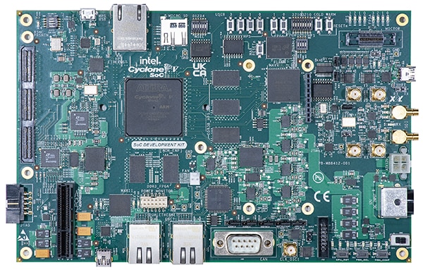
Developers can evaluate the Cyclone V SoC family using the DK-DEV-5CSXC6N-B Development Kit (Figure 2). This kit is designed for rapid prototyping of complex, high-throughput systems.
 Figure 2: The DK-DEV-5CSXC6N-B Cyclone V development kit supports high-performance prototyping. (Image source: Altera)
The kit includes several notable features:
- Dual Ethernet ports, a PCIe x4 connector, and a high-speed mezzanine card (HSMC) with 16 LVDS channels in each direction
- USB 2.0 OTG, CAN, UART, and a two-line text LCD interface
- 1 gigabyte (Gbyte) DDR3 SDRAM each for the FPGA and HPS sides, 128 megabytes (Mbytes) quad SPI Flash, and a 4 Gbyte microSD card
The board features the 5CSXFC5D6F31C8N device, which includes a dual-core Arm Cortex-A9 processor running at 600 MHz, with 85K LEs, 87 DSP blocks, and 288 I/O pins in a 31 mm × 31 mm, 896-FBGA package.
Power-efficient configurable logic in a compact package
Tight constraints around space and power consumption define many applications. Examples include sensor interfaces, power sequencing, and peripheral control. FPGAs such as the MAX 10 family offer an effective solution in these cases. MAX 10 devices are available in configurations from 2K to 50K LEs and packages as small as 3 mm × 3 mm.
Key features include up to two integrated 12-bit ADCs, a DDR3 memory interface, and multiplier blocks that support 18 × 18 and dual 9 × 9 fixed-point modes. On-chip Flash with support for dual image storage allows the FPGA to configure itself without an external memory device.
Power-saving capabilities are one of the MAX 10 family’s most distinctive attributes. A built-in sleep mode can reduce dynamic power consumption by up to 95%. Thanks to the on-chip Flash, devices can also be fully powered down and then resume operation in under 10 milliseconds (ms).
A single-supply option further simplifies power delivery. This makes MAX 10 devices especially well-suited to supervisory roles, where power domains may need to come online before the rest of the system.
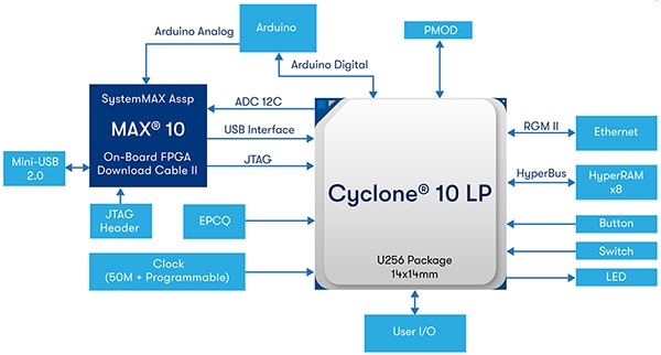
Developers interested in the MAX 10 can evaluate the family using the EK-10M08E144 MAX 10 FPGA evaluation board (Figure 3). This board provides access to external signals via Arduino UNO R3 connectors and test points, with a layout designed to support the measurement of ADC performance and overall power behavior.
 Figure 3: The EK-10M08E144 MAX 10 FPGA evaluation board provides easy access to key I/O. (Image source: Altera)
The board features the 10M08SAE144C8G device, which includes 8K LEs and a single ADC in a 144-pin LQFP package. In addition to its built-in hardware resources, this FPGA supports the RISC-V-based Nios V soft processor, enabling designers to implement lightweight control functions without needing an external microcontroller unit (MCU).
Balanced performance for mid-range applications
Some applications require more logic and I/O capacity than entry-level FPGAs can provide. Examples include sensor fusion, motion control, and chip-to-chip bridging. Cyclone 10 LP FPGAs address these requirements by offering up to 120K LEs and 525 I/O pins in devices optimized for balanced power and bandwidth in cost-sensitive applications.
Like the MAX 10, the family includes DSP blocks suitable for workloads such as filtering, control loops, and basic AI inferencing. Unlike the MAX 10, Cyclone 10 LP devices incorporate true LVDS transceivers and on-chip termination (OCT) to support high-speed digital interfacing.
Developers interested in the Cyclone 10 LP can evaluate the family using the EK-10CL025U256 Cyclone 10 evaluation kit (Figure 4). This board offers Arduino UNO R3 and Digilent Pmod connectors for easy expansion. Other features include GbE, USB 2.0, 128 megabits (Mbits) of SDRAM, and 64 Mbits of Flash memory.
 Figure 4: The EK-10CL025U256 Cyclone 10 evaluation kit supports easy peripheral expansion. (Image source: Altera)
The board features the 10CL025YU256C8G device, which includes 25K LEs, 66 DSP blocks, and 150 I/O pins in a 14 mm × 14 mm package. Like the MAX 10, the Cyclone 10 LP family supports the Nios V soft processor.
Conclusion
Designers now have more flexibility than ever when implementing custom logic in embedded systems. High-performance applications can benefit from FPGAs with integrated AI accelerators. Low-power designs can take advantage of devices with sleep modes. I/O-intensive systems can leverage chips with large pin counts and high-speed interfaces. Importantly, all these capabilities can be realized within the tight limitations of resource-constrained embedded systems with easy-to-use kits.

Disclaimer: The opinions, beliefs, and viewpoints expressed by the various authors and/or forum participants on this website do not necessarily reflect the opinions, beliefs, and viewpoints of DigiKey or official policies of DigiKey.


