How to Power and Protect Vehicle Asset Tracking Devices to Ensure Reliable Operation
Contributed By DigiKey's North American Editors
2022-09-15
Modern logistics and supply chain challenges can be helped by implementing vehicle asset tracking across fleets of commercial vehicles to ensure efficiency and effectiveness. However, designers of vehicle asset tracking devices need to design for ruggedness, harsh electrical environments, high levels of shock and vibration, and wide operating temperature ranges. At the same time, they must still meet increasing performance, efficiency, and protection requirements in smaller form factors with wider input voltage ranges—typically 4.5 to 60 volts direct current (dc).
The importance of protection cannot be overstated, given the operating conditions and asset value. It must typically include protection for overcurrent, overvoltage, undervoltage, and reverse voltage conditions to ensure reliable operation and support high levels of availability.
Designing the power conversion and protection circuitry needed to achieve these operational requirements from scratch can be challenging. While doing so can lead to a fully optimized design, it can also lead to delayed time to market, cost overruns, and compliance issues. Instead, designers can turn to off-the-shelf DC/DC converter power modules and protection ICs.
This article reviews the power requirements for vehicle asset tracking devices and outlines what a typical power management and protection architecture for those devices looks like. It then presents real-world DC/DC converter modules and protection ICs from Maxim Integrated Products that designers can use in these applications. Related evaluation boards and printed circuit board (PC board) layout guidelines are also provided.
Vehicle asset tracker power requirements
The vehicle battery is the primary power source for tracking devices and is usually 12 volts DC in consumer vehicles and 24 volts DC in commercial trucks. The asset trackers are sold as an aftermarket accessory and are expected to include a rechargeable backup battery that’s large enough to last a few days. In addition, these devices require protection from transient and fault conditions on the vehicle power bus, and they usually include a combination of step-down DC/DC converters and low drop-out regulators (LDOs) to power the system elements (Figure 1).
 Figure 1: The power system in a typical asset-tracking/fleet-management device includes two or more step-down DC/DC converters, an LDO, and a protection IC. (Image source: Maxim Integrated)
Since they are installed as an aftermarket item, asset tracking devices must be as small as possible to fit into available spaces. The power conversion components need to be highly efficient to enable longer device lifetime and longer backup from a relatively small battery. As asset tracking devices are generally in sealed enclosures, it’s important to minimize internal heat generation that could negatively impact lifetime and reliability. As a result, the power system must provide an optimal combination of miniaturization and high efficiency. While LDOs are compact, they aren’t the most efficient option.
Instead, designers can turn to synchronous buck DC/DC converters that deliver high conversion efficiencies. For example, 72% efficiency is a typical value for a 24-volt to 3.3-volt synchronous buck conversion, and 84% efficiency for a 24-volt to 5-volt conversion. The use of synchronous DC/DC converters results in lower thermal dissipation, contributing to higher reliability and the opportunity to use a smaller backup battery. The challenge is designing a compact solution with the 60-volt DC maximum input rating required in these applications.
Synchronous buck ICs vs. integrated modules
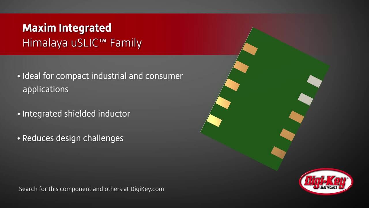
To achieve the design goals for small size and efficiency, designers can choose from solutions based on synchronous DC/DC converter ICs or integrated DC/DC converter modules. A typical 300 mA synchronous buck IC solution requires a 2-millimeter square (mm2) IC, an inductor that is about 4 mm2, plus several other passive components, occupying a total of 29.3 mm2 of PC board area. Alternatively, Himalaya μSLIC integrated synchronous buck modules from Maxim Integrated provide a solution that is 28% smaller, occupying only 21 mm2 of PC board area (Figure 2).
 Figure 2: Compared with a conventional buck converter implementation (left), a Himalaya μSLIC power module solution (right) occupies 28% less board space. (Image source: Maxim Integrated)
Going vertical
Himalaya μSLIC power modules vertically integrate the inductor and the buck converter IC, resulting in a significant reduction in PC board space compared to typical planar solutions. The μSLIC modules are rated for operation up to 60 volts DC input, and from -40 to +125°C. Even with vertical integration, they are still low profile and compact in a 10-pin, 2.6 x 3 x 1.5 high mm package (Figure 3).
 Figure 3: In a Himalaya μSLIC power module, the inductor is vertically integrated on the IC to minimize board space. (Image source: Maxim Integrated)
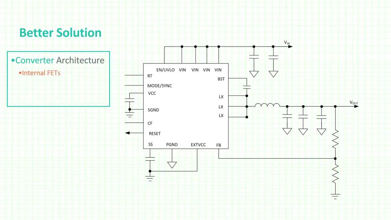
The MAXM15062/MAXM15063/MAXM15064 high-efficiency, synchronous buck modules include an integrated controller, MOSFETs, compensation components, and an inductor. They require only a few external components to implement a complete high-efficiency DC/DC solution (Figure 4). These modules can deliver up to 300 mA and operate over an input voltage range of 4.5 to 60 volts DC. The MAXM15064 has an output adjustable from 0.9 to 5 volts DC, while the MAXM15062 and MAXM15063 have fixed outputs of 3.3 and 5 volts DC, respectively.
 Figure 4: The MAXM15064 requires only three capacitors and two resistors to make a complete buck converter solution. (Image source: Maxim Integrated)
These modules have a peak-current-mode control architecture that offers the advantages of cycle-by-cycle current limiting, inherent short circuit protection, and good transient response. They have a fixed 4.1 millisecond (ms) soft start time to reduce inrush currents. Designers can turn to these efficient buck converter modules to streamline the design process, reduce manufacturing risks, and speed time to market.
Evaluation kits show proven designs
The MAXM15064EVKIT# evaluation kit provides a proven design to evaluate the MAXM15064 synchronous buck module (Figure 5). It is programmed to deliver 5 volts DC for loads up to 300 mA. It features an adjustable input undervoltage lockout, open-drain RESET signal, and a selectable pulse width modulation (PWM) or pulse frequency modulation (PFM) mode. PFM mode can be used to deliver higher light-load efficiency. It complies with CISPR22 (EN55022) Class B conducted and radiated emissions and delivers 78.68% efficiency with a 48-volt DC input and an output of 200 mA.
 Figure 5: The MAXM15064EVKIT# is a 5-volt DC output evaluation kit for the MAXM15064 that can deliver up to 300 mA. (Image source: Maxim Integrated)
Protection ICs
Designers can use the MAX176xx adjustable overvoltage and overcurrent protection ICs along with the MAXM1506x synchronous buck modules for a complete system solution. These ICs are in a 12-pin TDFN-EP package and are designed to protect systems from negative and positive input voltage faults from -65 to +60 volts. They have an internal field effect transistor (FET) with a typical on resistance (RON) of just 260 milliohms (mΩ). The input overvoltage protection range is programmable from 5.5 to 60 volts, while the input undervoltage protection range is adjustable from 4.5 to 59 volts. External resistors are used to set the input overvoltage-lockout (OVLO) and undervoltage-lockout (UVLO) thresholds.
The current limit protection is programmable with a resistor up to 1 ampere (A) to help control inrush currents when charging large output filter capacitors. The current limit can be implemented in three modes; auto retry, latch-off, or continuous. The voltage on the SETI pin is proportional to the instantaneous current and can be read by an analog-to-digital converter (ADC). These ICs have an operating temperature range of -40 to +125°C and include thermal shutdown to protect from excessive temperatures. An optional surge suppressor device can be used in applications that anticipate high input surge currents (Figure 6). There are three ICs in the family:
- The MAX17608 protects against overvoltage, undervoltage, and reverse voltage.
- The MAX17609 protects against overvoltage and undervoltage.
- The MAX17610 protects against reverse voltage.
 Figure 6: Typical integration of the MAX17608 and MAX17609 protection ICs showing the optional surge suppressor (left) for high input surge applications. (Image source: Maxim Integrated)
Evaluation kits for protection ICs
The MAX17608EVKIT, the MAX17609EVKIT, and the MAX17610EVKIT enable designers to evaluate the performance of the MAX17608, MAX17609 and MAX17910, respectively (Figure 7). For example, the MAX17608EVKIT is a fully assembled and tested circuit board for evaluating the MAX17608. It is rated for 4.5 to 60 volts and 1 A, with under voltage, overvoltage, reverse-voltage protection, and forward/reverse current limit. The MAX17608EVKIT can be configured to demonstrate adjustable undervoltage and overvoltage protection, three current limit modes, and various current limit thresholds.
 Figure 7: Evaluation boards such as the MAX17608EVKIT# for the MAX17608, are also available for the MAX17609 and MAX17610 protection ICs. (Image source: Maxim Integrated)
PC board layout guidelines
When laying out the MAX1506x and MAX176xx, some basic guidelines should be adhered to for a successful design. For example, for the MAX1506x:
- Input capacitors should be as close as possible to the IN and GND pins.
- The output capacitor should be as close as possible to the OUT and GND pins.
- The feedback (FB) resistor dividers should be as close as possible to the FB pin.
- Use short power traces and load connections.
For the MAX176xx:
- Keep all traces as short as possible; this minimizes any parasitic inductances and optimizes the switch response time to output short circuits.
- Input and output capacitors should be no more than 5 mm away from the device; closer is better.
- The IN and OUT pins must be connected to the power bus with short, wide traces.
- The use of thermal vias from the exposed pad to the ground plane is recommended to improve thermal performance, especially for continuous current limit mode.
For reference, Figure 8 shows both the MAXM17608 and MAXM15062 and their respective positions in the power chain.
 Figure 8: A typical asset tracking device block diagram showing where synchronous buck converters and protection ICs from Maxim Integrated fit. (Image source: Maxim Integrated)
Conclusion
As shown, designers can turn to the MAX1506x high-efficiency, synchronous buck modules and the MAX176xx protection ICs to implement a complete power and protection solution for vehicle asset tracking devices. Following core best practices during implementation, the resulting solution can be efficient, compact, and rugged, while minimizing manufacturing risks and compliance issues.
Recommended Reading
Disclaimer: The opinions, beliefs, and viewpoints expressed by the various authors and/or forum participants on this website do not necessarily reflect the opinions, beliefs, and viewpoints of DigiKey or official policies of DigiKey.