How to Drive SiC MOSFETs and IGBTs with Precision, Efficiency, and Protection
Contributed By DigiKey's North American Editors
2025-03-12
As power systems evolve to meet the demands of electric vehicles (EVs), renewable energy, and industrial automation, it is becoming more challenging for designers to balance efficiency, performance, and safety. While the integration of high-voltage components such as insulated-gate bipolar transistors (IGBTs) and silicon carbide (SiC) metal-oxide-semiconductor field-effect transistors (MOSFETs) is a critical step toward achieving this balance, these devices require gate drivers that can deliver precise control, rapid switching, and robust protection mechanisms.
This article explores the challenges associated with driving modern power systems, emphasizing half-bridge topologies. It then introduces gate drivers and an evaluation board from Infineon Technologies that can help overcome these challenges.
Design challenges for modern half-bridge topologies
Power systems face mounting challenges as the industry pushes toward higher switching frequencies, elevated voltages, and the adoption of wide-bandgap (WBG) semiconductors. While these advancements enable greater efficiency, they place heavy demands on gate drivers.
Consider the half-bridge topology, which has become standard across many applications, to illustrate the escalating requirements. Half-bridge circuits are essential in EV DC-to-DC onboard chargers and motor drive systems. They enable bidirectional power flow, which is critical during both normal motor operation (forward power flow) and regenerative braking (reverse power flow). The transition to 800 V architectures in newer EV platforms intensifies the need for reliable isolation and protection mechanisms while maintaining switching precision.
For renewable energy systems, half-bridge designs are foundational to the three-phase inverters required for grid integration. The higher switching frequencies used with SiC MOSFETs and IGBTs increase efficiency but exacerbate common-mode voltage issues on both high-side and low-side switches, generating significant electromagnetic interference (EMI) that can compromise system performance and potentially violate regulatory standards.
Industrial motor drives face additional challenges, including maintaining balanced DC bus voltage across split capacitor arrangements. The trend toward more compact, higher power density designs increases thermal management difficulties and electrical noise concerns.
Across all these applications, designers need gate driver solutions that deliver precise control, rapid switching capabilities, and comprehensive protection features while providing robust isolation between high and low-voltage circuits.
A dual-channel gate driver built for IGBTs and MOSFETs
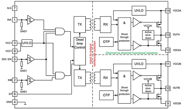
Infineon Technologies’ EiceDRIVER 2ED314xMC12L series (Figure 1) addresses these challenges with a dual-channel design engineered to control IGBTs and MOSFETs. All series members offer independent channel operation with dead-time control (DTC) to allow the 2ED314xMC12L device to operate as a dual-channel low-side driver, a dual-channel high-side driver, or a half-bridge gate driver.
 Figure 1: The 2ED314xMC12L series features independent channel operation with DTC, allowing the devices to operate as dual-channel low-side drivers, dual-channel high-side drivers, or half-bridge gate drivers. (Image source: Infineon Technologies)
In a half-bridge configuration, the dual-channel architecture allows a single gate driver IC to control both high-side and low-side switches efficiently. This integration simplifies printed circuit board (pc board) layout, reduces component count, and supports matched timing characteristics between channels, which is critical for maintaining proper DTC and preventing shoot-through conditions.
A key advantage of the 2ED314xMC12L series is its galvanic isolation through coreless transformer technology. This approach delivers fast signal transmission with high immunity to EMI, which is essential in electrically noisy environments like EVs.
The isolation capability is certified to UL 1577 standards, providing 6.84 kV root mean square (kVRMS) for 1 second and 5.7 kVRMS for 1 minute. This robust isolation level is crucial to protect against high-voltage transients in applications such as renewable energy systems, where grid-tie inverters must withstand utility-scale voltage surges.
High-output, high-precision switching
The 2ED314xMC12L series performs well on several relevant benchmarks, starting with its 6.5 A peak output current. This high output is particularly beneficial for SiC MOSFETs, which require strong gate-drive signals for efficient switching.
Another key characteristic is a propagation delay of 39 ns, which enables precise timing control. This is an important consideration for applications such as industrial automation, where motor speed and torque control depend on high-precision switching.
A tight part-to-part propagation delay skew of 8 ns maximum means that when using multiple driver ICs, such as in a three-phase motor drive, the timing differences between the parts will be minimal. An even tighter channel-to-channel propagation delay skew of 5 ns maximum helps prevent shoot-through between switches for each half-bridge.
Finally, a common-mode transient immunity (CMTI) rating of more than 200 kV per microsecond (kV/µs) helps prevent false triggering due to voltage transients. In renewable energy applications, for example, high transient immunity supports stable operation during grid fluctuations and sudden shifts in power flow.
Reliability features for steady operation
The 2ED314xMC12L series incorporates multiple protection features to ensure reliable operation in demanding power applications. Each feature addresses specific reliability concerns that arise in high-voltage switching environments.
Necessary safeguards are active shutdown and short-circuit clamping. These mechanisms protect against shoot-through currents in half-bridge configurations where the two power switches are stacked between the DC bus voltage. If both switches were to turn on simultaneously, the resulting short circuit could damage components or shut down the system.
Another notable feature is undervoltage lockout (UVLO) protection, which creates a hysteresis “dead band” where the state remains stable despite small voltage fluctuations, preventing oscillation at the threshold. In solar power systems, for example, UVLO provides steady operation under partly cloudy conditions, avoiding unnecessary disruptions. Some variants offer UVLO between 8.5 V and 9.3 V, while others provide protection between 12.5 V and 13.6 V.
Options are also available with an enable pin, which adds an extra layer of control for emergency shut down situations. In these variants, each digital input pin includes a pull-down resistor, ensuring that if a pin is desoldered or disconnected, it defaults to a safe state with the channel disabled. This feature is particularly relevant in high-reliability applications where system integrity must be maintained even in the event of unexpected faults.
Variants with disable pins are available for applications prioritizing lower current consumption and simplified control. These models allow the gate driver to remain active by default, reducing standby power consumption and simplifying system design.
Examples of the options available are the 2ED3140MC12L, which offers UVLO with hysteresis between 8.5 V and 9.3 V and a disable pin. In contrast, the 2ED3146MC12L provides UVLO between 12.5 V and 13.6 V and an enable pin.
Efficient yet reliable packaging
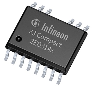
The series is offered in a PG-DSO-14-71 package (Figure 2). This surface-mount package measures 10.3 x 7.5 millimeters (mm), notably compact dimensions for a high-power, dual-channel driver. In EV applications, this package saves valuable powertrain space.
 Figure 2: The 2ED314xMC12L series is offered in a compact PG-DSO-14-71 package. (Image source: Infineon Technologies)
Despite their small size, all variants provide sufficient spacing for safe operation: 8 mm input-to-output and 3.3 mm channel-to-channel creepage and clearance distances. These dimensions satisfy isolation requirements while maintaining the compact form factor needed in space-constrained designs.
Get a quick start with an evaluation board
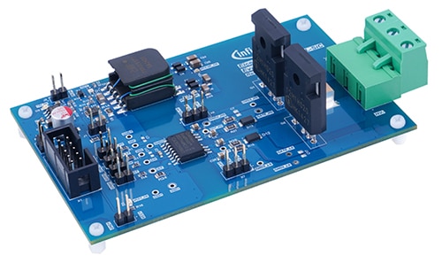
To streamline testing and development, Infineon Technologies offers the EVAL-2ED3146MC12L evaluation board (Figure 3). This half-bridge board is designed to showcase the functionality and capabilities of the 2ED3146MC12L isolated gate driver IC.
 Figure 3: The EVAL-2ED3146MC12L evaluation board provides a half-bridge setup to evaluate the 2ED3146MC12L. (Image source: Infineon Technologies)
Beyond the gate driver, the evaluation board includes two Infineon Technologies IMZA120R020M1HXKSA1 CoolSiC trench MOSFETs, as well as an Infineon Technologies 2EP130R transformer driver IC for the onboard power supply. These components are suitable for evaluation purposes and represent practical choices for real-world designs.
The SiC MOSFETs feature a 1,200 V drain-to-source voltage rating, well within the 2ED314xMC12L’s capability to drive 600 V to 2,300 V power devices. These MOSFETs’ gate-drive voltage requirements of 18 V are comfortably accommodated by the 2ED314xMC12L’s 35 V absolute maximum output supply voltage. The MOSFETs’ low on-state resistance of 19 mΩ at +25°C minimizes conduction losses.
With a maximum power dissipation capability of 375 W at +25°C and an operating temperature range of -55°C to +175°C, these MOSFETs align with the requirements of high-performance power electronic applications. The gate driver’s fast 39 ns propagation delay and high CMTI of >200 kV/μs enable efficient high-frequency switching while maintaining reliable operation across the MOSFETs’ full temperature range.
The 2EP130R transformer driver complements the gate driver with its wide switching frequency range of 50 to 695 kilohertz (kHz), working in concert with the 2ED3146MC12L’s fast propagation delay. The transformer driver’s high-accuracy duty cycle adjustment (10% to 50%) pairs well with the gate driver’s precise timing characteristics, a crucial combination for maintaining optimal dead time in half-bridge configurations.
Conclusion
Infineon Technologies’ EiceDRIVER 2ED314xMC12L series delivers the balance of efficiency, performance, and safety features necessary for high-voltage applications in EVs, renewable energy, and industrial automation. Its compact PG-DSO-14-71 package supports space-constrained designs, while the EVAL-2ED3146MC12L-SiC evaluation board enables quick testing.

Disclaimer: The opinions, beliefs, and viewpoints expressed by the various authors and/or forum participants on this website do not necessarily reflect the opinions, beliefs, and viewpoints of DigiKey or official policies of DigiKey.


