How to Design and Certify Functionally Safe RTD-Based Systems
Contributed By DigiKey's North American Editors
2023-07-24
A resistance temperature detector (RTD), consisting of a transducer and its analog front-end (AFE) signal conditioning circuit, is widely used, accurate, and reliable. However, for mission-critical and high-reliability applications, it is often necessary to design and ensure a functionally safe system via the Route 1S or Route 2S component certification process.
Certifying a system for functional safety is a complex process, as all components in the system must be reviewed for potential failure modes and mechanisms. There are various methods to diagnose failures and using parts that are already certified eases this workload along with the certification process.
Note that “reliability” is related to but is not the same as functionally safe. In its simplest terms, reliable refers to a design and implementation which works to specifications without problems or failure, while “functionally safe” means that any failures must be detected by the design. Both reliability and functional safety are needed for critical applications.
This article will look at the basics of RTDs and their signal conditioning circuitry in the context of functionally safe certification. It will then discuss the various levels of reliability and failure certification, and what is required to meet them via both routes. Two multichannel RTD AFE ICs, the AD7124 pair from Analog Devices, along with an associated evaluation board arrangement, will be used to illustrate the key points.
The role of functional safety
The role of functional safety is to provide freedom from unacceptable risk of injury or damage to the health of people through the proper implementation of one or more automatic protection/safety functions. It ensures that the product, device, or system continues to function safely if there is a malfunction. It is needed in a wide span of industrial, commercial, and even some consumer applications, such as:
- Autonomous vehicles
- Machine safety and robotics
- Industrial control systems (ICS)
- Consumer smart home products
- Smart factories and supply chains
- Safety-instrumented systems and hazardous-location control systems
For example, in a functionally safe design, the function of a master power on/off switch would still support power shut off, even if other components in the system failed (Figure 1).
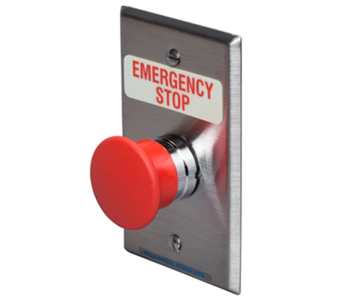 Figure 1: In a functionally safe system, there can be no doubt or ambiguity that this switch will do what it says it is designed to do. (Image source: Pilla via City Electric Supply Co.)
RTD basics
Why look at temperature and functional safety? One good reason is that temperature is the most commonly measured physical parameter. It is often related to safety or critical applications, and it is supported by a wide selection of transducers. Among these are RTDs, which are conceptually simple: they leverage the known and repeatable temperature coefficient of resistance (TCR) of metals such as nickel, copper, and platinum. Platinum RTDs with 100 ohm (Ω) and 1000 Ω resistance at 0°C are the most widely used and can be used over the range of -200°C to +850°C.
These RTDs have a highly linear resistance-versus-temperature relationship over this temperature range; for ultra-high accuracy situations, there are correction and compensation tables and factors that can be applied. The platinum RTD with a nominal 100 Ω resistance (designated as PT100) has a typical resistance of 18 Ω at -200°C and 390.4 Ω at +850°C.
Using an RTD requires that it be excited by a known current that is usually kept to around 1 milliamp (mA) to minimize self-heating. Other current values are also used, depending on the nominal RTD resistance.
The voltage drop across the RTD is simultaneously measured via an AFE consisting of a programmable-gain amplifier (PGA), and in almost all cases, an analog-to-digital converter (ADC) in conjunction with a microcontroller unit (MCU) (Figure 2).
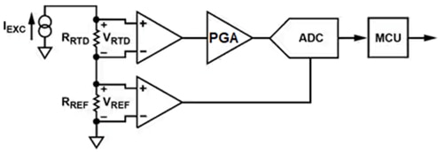 Figure 2: Using an RTD to measure temperature requires the driving of a known current through the RTD and measuring the voltage drop across it, then applying Ohm’s law. (Image source: Digi-Key)
The circuit topology of this basic scheme is identical to the use of a sense resistor to determine current through a load, but here the known and unknown variables are switched. For current sensing, the resistance is known while the current is unknown, so the calculation is I = V/R. For RTDs, the current is known, but the resistance is not, so the calculation is R = V/I.
The PGA is needed to maintain signal integrity and maximize dynamic range, as the voltage levels across the RTD can range from tens of millivolts to hundreds of millivolts, depending on the RTD type and temperature.
The physical connection between the excitation source, the RTD, and the PGA can be a two, three, or four-wire interface. While two leads are sufficient in principle, there are issues associated with IR drop in the connection leads, along with other artifacts. Using the three and four-wire topologies in a more advanced Kelvin connection results in more accurate and consistent performance, even though it adds to wiring costs (Figure 3).
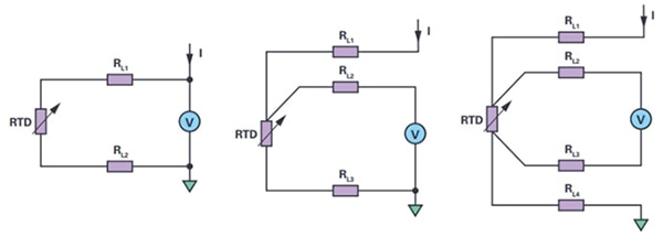 Figure 3: The RTD can be driven and sensed via just two wires (left), but the use of three leads (center) and even four leads (right, Kelvin connection) enable the elimination of various error sources due to the leads. (Image source: Analog Devices)
Begin with terminology and standards
As with many specialties, functional safety has many unique terms, data sets, and acronyms that are widely used in related discussions. Among these are:
- Failures in time (FIT): the number of failures that can be expected in one billion (109) hours of device operation.
- Failure modes and effects analysis (FMEA): the process of reviewing as many components, assemblies, and subsystems as possible to identify potential failure modes in a system, and their causes and effects.
- Failure modes effects and diagnostic analyses (FMEDA): A systematic analysis technique to obtain subsystem/product level failure rates, failure modes, and diagnostic capability.
FIT data is needed along with failure modes effects and diagnostic analyses (FMEDAs) on the different components in the system for full analysis. FMEA only offers qualitative information, while FMEDA offers both qualitative and quantitative information, allowing users to measure a level of criticality to failure modes and order them according to importance. FMEDA adds risk, failure modes, effects and diagnostics analysis, and reliability information.
- Safety Integrity Level (SIL): There are four discrete integrity levels associated with SIL: SIL 1, SIL 2, SIL 3, and SIL 4. The higher the SIL level, the higher the associated safety level, and the lower probability that a system will fail to perform properly.
A SIL 2 rating indicates that over 90% of failures within the system can be diagnosed. To certify a design, the system designer must provide evidence to the certification house on the potential failures, whether these are safe failures or hazardous failures, and how the failures can be diagnosed.
- IEC 61508, formally titled “Functional Safety of Electrical/Electronic/Programmable Electronic Safety-related Systems” (and informally called just “Electronic Functional Safety”), is the specification for functionally safe designs. It documents the design flow needed to develop a SIL-certified part. Documentation needs to be generated for each step, from concept and definition to design, layout, fabrication, assembly, and test.
This process is known as Route 1S and is complicated. However, there is an alternative to Route 1S called the Route 2S flow. This is a “proven in use” route and is applicable when large volumes of the product have been designed into end products and systems and are being used in the field with thousands of hours of accumulated operation.
Under Route 2S flow, a product can still be certified by providing evidence to the certification authority of:
- Volumes used in the field
- Analysis of any returns from the field and detail that the returns were not due to failures within the component itself
- Safety datasheet giving detail on the diagnostics and the coverage they provide
- Pin and die FMEDA
Merging RTD interfaces with SIL Route 2S flow
Certifying a system is a long process, as all components in the system must be reviewed for potential failure mechanisms, and there are various methods to diagnose failures. Using parts that are already certified reduces the effort required and shortens the certification process.
A highly integrated, mature RTD interface component is key to easing Route 2S certification, as it defines a complete solution package and thus can be fully characterized with data associated with field use and failures. This is unlike the use of multiple smaller building-block ICs, where their various interfaces and interactions must be analyzed for the specific interconnection configuration being used.
An example of this is the four-channel AD7124-4 (Figure 4), and the similar eight-channel AD7124-8 (henceforth referred to collectively as the “AD7124” when discussing the many features they have in common). These components are a good fit for the Route 2S flow due to their embedded self-test and diagnostic features, as well as their “track record” in the field.
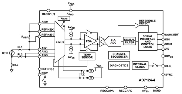 Figure 4: The four-channel AD7124-4 is a functionally complete RTD sensor-to-processor signal chain. (Image source: Analog Devices)
These ICs are complete solutions for multichannel RTD measurement and include all the building blocks needed from a sensor to a digitized output and for communication with an associated microcontroller. They include the multichannel multiplexer, PGA, 24-bit sigma-delta ADC, current sources for the RTDs, voltage references for internal operation, system clock, analog and digital filtering, and three-wire or four-wire serial interfaces for SPI, QSPI, MICROWIRE, and DSP-compatible interconnections.
However, the presence of these functions does not inherently provide a basis for SIL Route 2S qualification. For a functionally safe design, an array of embedded diagnostics are required for the many functions that comprise the RTD system. The multiple embedded diagnostics in the AD7124 minimize both the design complexity and design time, and remove the need to duplicate the signal chain for diagnostic coverage.
These diagnostics include, but are not limited to, monitoring of the power supply, reference voltage, and analog input; detection of an open wire to the RTDs; checking of conversion and calibration performance; checking the functionality of the signal chain; monitoring of the read/write functions; and monitoring of the register contents.
How do these “high level” statements translate into the necessary on-chip diagnostics? There are many facets to the answer, including:
SPI Diagnostics: For every write to the AD7124, the processor generates a cyclic redundancy check (CRC) value that is appended to the information being sent to the ADC. The ADC then generates its own CRC value from the information received and compares it to the CRC value received from the processor. If both values agree, the information is intact and will be written to the relevant on-chip register.
If the values do not match, this means a bit of corruption has occurred in the transmission, and the IC sets an error flag that indicates that data corruption has occurred. The AD7124 also self-protects by not writing the corrupt information into a register.
A similar CRC procedure is used when information is being read from the AD7124 to the system processor. Finally, the interface also counts clock pulses to ensure that there are just eight such pulses with each read or write data frame, thus ensuring that a clock glitch has not occurred.
Memory checks: A CRC is also used to validate register contents on power-up or whenever on-chip registers are altered (such as when changing the gain). The CRC process is also executed periodically to ensure that no memory bit has “flipped” due to noise or other causes. If there is a change and the processor is subsequently flagged that the register settings have been corrupted, it can reset the ADC and reload the registers.
Signal Chain Checks: All critical static voltages can be checked via the ADC, including power supply rails, low-dropout (LDO) regulator outputs, and reference voltages; the presence or absence of the external capacitor across the LDO can also be checked. In addition, a known voltage can be applied to the ADC input to check the ADC and the gain-function settings. Further, known currents can be injected across the analog inputs to check for an open or shorted RTD.
Conversion and calibration: The results of the ADC conversion are continuously checked to see if they go to all zeroes or full scale, either of which indicates a problem. The bit stream from the modulator at the core of the ADC is monitored to ensure that it has not saturated, and if saturation occurs (meaning there have been 20 consecutive ones or zeroes from the modulator), an error flag is set.
Master clock frequency: The frequency of this clock not only controls conversion rates but also establishes the notch frequencies of the 50/60 Hertz (Hz) digital filters. An internal register in the AD7124 allows the companion processor to time and thus check the accuracy of the master clock.
Additional features: The AD7124 includes a temperature sensor, which also can be used to monitor the die temperature. Both versions have a 4 kilovolt (kV) electrostatic discharge (ESD) rating for robust performance, and both are housed in a 5 × 5 millimeter (mm) LFCSP package that is suitable for intrinsically safe designs.
Due to the internal complexity, sophistication, and advanced self-test features of the AD7124-4 and AD7124-8, it makes sense to have a means by which to exercise and evaluate the ICs.
To achieve this, Analog Devices offers a pair of connected boards: the EVAL-AD7124-4SDZ evaluation board for the AD7124-4 (Figure 5), and the companion EVAL-SDP-CB1Z SDP (System Demonstration Platform)/Interface Board (Figure 6). The former is specific to the AD7124-4 and works in conjunction with the latter, which provides communication with the user’s PC and evaluation software via a USB link.
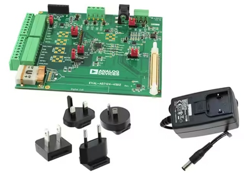 Figure 5: The EVAL-AD7124-4SDZ is an evaluation board for the AD7124-4. (Image source: Analog Devices)
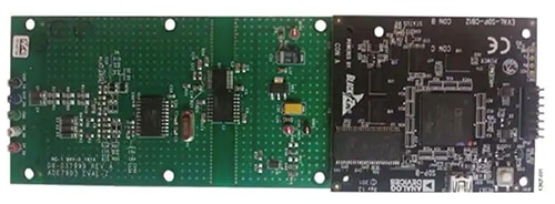 Figure 6: The EVAL-SDP-CB1Z/Interface Board is a companion to the EVAL-AD7124-4SDZ evaluation board, providing a USB connection to a host PC. (Image source: Analog Devices)
The evaluation arrangement is supported by the AD7124-4 EVAL+ software, which fully configures the AD7124-4 device register functionality and exercises the IC. It also provides time-domain analysis in the form of waveform graphs, histograms, and associated noise analysis for ADC performance evaluation.
Transition to functionally safe design
It’s important to realize that the AD7124-4 and AD7124-8 are not SIL rated, meaning that they are not designed and developed using development guidelines as defined by the IEC 61508 standard. However, by understanding the end application and through the appropriate use of the various diagnostics, they can be assessed for use in a SIL-rated design.
The path to Route 1S certification has multiple considerations for analyzing and addressing failures, which can be systemic or random. Systemic failures are due to design or manufacturing shortcomings, such as a noisy interrupt due to a lack of filtering on the external interrupt pin or insufficient headroom for a signal. In contrast, random failures are due to physical causes such as corrosion, thermal stress, or wear-out.
An important concern is called the dangerous undetected failure, which is addressed by multiple techniques. To minimize random failures, designers use one or all of three tactics:
- More-reliable, less-stressed components.
- Diagnostics that rely on built-in detection mechanisms implemented via hardware or software.
- Fault tolerance via redundant circuitry. By adding a redundant path, a single failure can be tolerated. This is called a Hardware Fault Tolerance 1 (HFT 1) system, meaning that one failure cannot cause the system to fail.
One tool to understand SIL level coverage is a matrix that plots safe failure fraction (SFF) (the amount of diagnostic coverage) and hardware fault tolerance (the redundancy) (Figure 7).
|
|||||||||||||||||||||||
Figure 7: This matrix characterizes safe failure fraction (SFF) versus hardware fault tolerance (HFT) and provides insight into SIL coverage. (Image source: Analog Devices)
The rows show the amount of diagnostic coverage, while the columns show the hardware fault tolerance. An HFT of 0 means that if there is one fault in the system, the safety function will be lost. A higher level of diagnostics reduces the needed amount of system redundancy or improves the SIL level of the solution with the same level of redundancy (moving down the matrix).
Note that the FMEDA of a typical temperature application using these devices shows a safe failure fraction (SFF) greater than 90% according to IEC 61508. Two traditional ADCs would normally be required to provide this level of coverage via redundancy, but the AD4172 only requires a single ADC, thus providing significant savings in bill of materials (BOM) cost and board real estate.
Documentation for SIL-rated designs
Extensive documentation is needed to achieve Route 1S certification. Among the necessary source documents are:
- Safety datasheet (the safety manual for a SIL-rated part)
- Pin FMEDA and die FMEDA, with failure modes, effects, and analysis for both
- Annex F checklist (defined by IEC 61508)
This documentation, in turn, comes from a variety of sources (Figure 8):
- Diagnostic data from the datasheet captures all the diagnostic features available in the part.
- Design data refers to internal data. For example, the die area and impact of each internal block of the part.
- FIT, with rates for various components, are available from the data book.
- Fault insertion tests are done for blocks that cannot be analyzed using design and diagnostic data. These tests are planned based on the application requirements, and the outcome of fault insertion tests is used to strengthen the FMEDA and FMEA documents.
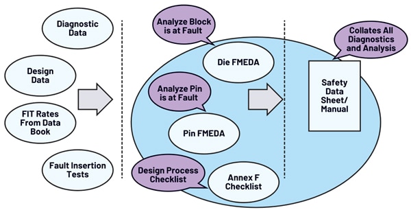 Figure 8: The diverse documentation sources are aggregated and pulled through to provide the complete information package needed for SIL certification. (Image source: Analog Devices)
Looking at specifics in more detail:
- The Safety Manual or Safety Datasheet uses all of the compiled information to provide the necessary requirements to enable the integration of the AD7124-4 or AD7124-8. It collates all the diagnostics and analyses that flow in from various documents and data sets.
- The die FMEDA for the AD7124-4 and AD7124-8 analyzes the main blocks in the application schematic, identifies failure modes and effects, and checks the diagnosis and analyses for a particular safety function. For example, the analysis of the clock module shows the failure modes, the effect of each on output, the amount of diagnostic coverage, and an analysis of the impact (Figure 9).
|
Figure 9: This table defines the master clock block failure mode, effects, diagnostics, and analysis. (Image source: Analog Devices)
This die FMEDA results in a quantitative presentation of failure rates for safe failures, dangerous detected failures, and dangerous undetected failures. All these are used to calculate the SFF.
The pin FDEMA looks at failures from a different perspective. It analyzes various types of failures on the pins of the AD7124-4 and AD7124-8 and their outcome for the RTD application. It does this for every individual pin and describes the outcome for the case where the pin opens up, shorts to supply/ground, or shorts to adjacent pins.
The Annex F Checklist is a design-measures checklist for the avoidance of systematic failures. It comprises:
- Product overview
- Application information
- Safety concept
- Lifetime predictions
- FIT
- FMEDA calculations—SFF and DC
- Hardware safety mechanisms
- Diagnostics description
- EMC robustness
- Operation in redundant configurations
- Annexes and document list
In summary, the functional safety certification for a newly introduced component via Route 1S is long, complex, time-consuming, intense, and comprehensive. Fortunately, Route 2S, as mentioned above, is an alternative approach that is viable for some components.
Route 2S: An alternative path
The path known as Route 2S is applicable for a released part with field experience and data and is designated as “proven in use.” It is based on an analysis of customer returns and the number of devices shipped. It cannot be used with new parts which have little or no exposure “track record” in actual use.
Route 2S allows SIL certification as if the part was fully analyzed under the IEC 61508 standard. It is available to module and system designers if they have successfully used the subject IC in the past and know the failure rate from the field. The embedded test and verification features, along with performance data, make the AD7214-4 and AD7214-8 good candidates for Route 2S.
Invoking Route 2S requires detailed and statistically significant data on field returns and failures. This requirement is much harder for IC vendors to meet than it is for board or module suppliers. The reason is that the former generally do not have enough knowledge of the final application, or what percentage of the failing units from the field are returned to them for analysis.
Conclusion
The Route 1S path for functionally safe certification of new products is thorough, comprehensive, and detailed. It is also technically challenging and definitely time-consuming. In contrast, the Route 2S process allows released products to be certified based on field experience, failures, and analysis data. This is a useful route that is supported by the AD7214-4 and AD7214-8 RTD interface ICs as they have the required history. Equally important, these ICs embed many diagnostic and self-test functions and features that make them suitable candidates for such certification.
Related Content

Disclaimer: The opinions, beliefs, and viewpoints expressed by the various authors and/or forum participants on this website do not necessarily reflect the opinions, beliefs, and viewpoints of DigiKey or official policies of DigiKey.


