How to Achieve Efficient Power Control in Space-Constrained Designs
Contributed By DigiKey's North American Editors
2023-06-13
Wearable devices like earbuds, smart watches, augmented reality (AR)/virtual reality (VR) glasses, and hearing aids are getting smaller and more discrete. At the same time, these applications demand greater functionality, including artificial intelligence (AI) capabilities. These trends create thermal management issues for designers. In addition, longer battery life is needed for a positive user experience, so high-efficiency designs are necessary. Balancing this mix of often conflicting design requirements is challenging designers to rethink component choices in order to minimize board space while maximizing time between charges.
To assist designers, miniature MOSFETs with very low “on” resistance have emerged. These devices also provide excellent thermal conductivity to help control heat dissipation. Some devices go so far as to embed electrostatic discharge (ESD) protection.
This article briefly discusses the challenges facing designers of small, smart, battery-powered devices. It then shows how these challenges can be resolved using miniature packaged MOSFETs from Nexperia, highlighting the devices’ characteristics and their applicability in micro-wearable designs.
The challenges of micro-wearable device design
Digital watches, earbuds, and smart jewelry, along with other miniature wearable devices, pose several challenges for designers, particularly with respect to size, power consumption, and thermal management. The challenges are only growing as higher levels of functionality, such as AI, are being offered to engage end users. Along with finding room for microcontrollers, batteries, Bluetooth transceivers, speakers, and display electronics, designers must now add a neural processing capability.
With increasing functionality comes the need for advanced power consumption minimization approaches to extend battery life. Control of power consumption includes turning off circuit elements that aren’t being used, but those circuits must be ready to turn on quickly when needed. While turning the power on and off is effective, it requires low on resistance within the switching devices to reduce power losses and generated heat. The effective management of any heat generated is complicated by the compact form factor of these devices, which only goes to underscore the importance of high-efficiency, low-loss components.
Drawing on its decades of experience in the production of discrete semiconductor components, Nexperia has been able to shrink the size of its MOSFETs to meet these often-conflicting demands in its DFN (discrete flat no lead) series (Figure 1).
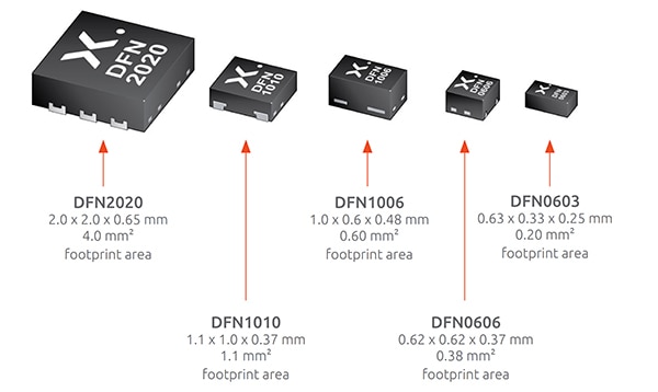 Figure 1: Shown is the Nexperia family of DFN-packaged MOSFET devices, highlighting the reduction in size and footprint, down to the DFN0603. (Image source: Nexperia)
The DFN0603 comes in a package measuring 0.63 by 0.33 by 0.25 millimeters (mm). The most significant change from the earlier model shown is the reduction in height down to 0.25 mm—without any decrease in functionality. In addition, the device features a drain-to-source on resistance (RDS(on)) that is 74% less than the earlier package.
This new ultra-low-profile package series includes five MOSFET devices, both N-channel and P-channel, rated at 20 to 60 volts drain-to-source voltage (VDS).
In addition to lower power dissipation enabled by their lower on resistance, the DFN0603 product line exhibits excellent thermal conduction, which keeps the temperature of the mounted device low.
Trench MOSFETs
This reduction in size, along with the reduction in RDS(on), is enabled by the device’s trench MOSFET design (Figure 2).
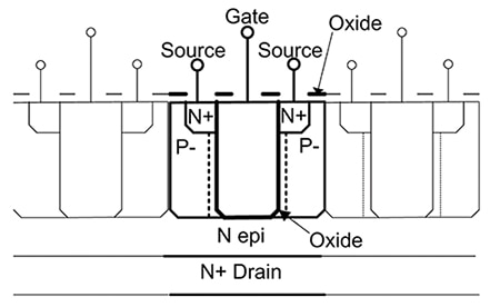 Figure 2: A cross-sectional view shows the structure of a trench MOSFET with current flowing vertically between the source and the drain when the device is in the on state. The dashed line shows the channel areas. (Image source: Art Pini)
Like other MOSFETs, a trench MOSFET cell has a drain, gate, and source, but the channel forms vertically, parallel to the gate trench, by means of the field effect. As a result, the direction of the current flow is vertical, from source to drain. Compared to a planar device, which is spread horizontally and takes a good deal of surface area, this structure is very compact, permitting a very large number of adjacent cells in the silicon die. All the cells are connected to work in parallel in order to reduce the value of RDS(on) and increase the drain current.
The Nexperia DFN0603 MOSFET family
The Nexperia DFN0603 series includes five devices—four N-channel MOSFETs and a single P-channel MOSFET (Figure 3), with VDS limits of 20 to 60 volts. All use the same physical package that has a total power dissipation limit of 300 milliwatts (mW).
|
||||||||||||||||||||||||||||||||||||||||||||||||||||||||||||||||||||||||||||||||||||||||||||||||||||
Figure 3: Shown are the specifications for five DFN0603 ultra-low-power MOSFETS intended for mobile and portable applications. (Image source: Nexperia)
Where:
VDS = The maximum drain-to-source voltage, in volts.
VGS = The maximum gate-to-source voltage, in volts.
ID = The maximum drain current in amperes.
VGSth = The minimum and maximum gate-to-source threshold voltages. This is the voltage required across the gate and source terminals to start to turn the MOSFET on. The minimum and maximum values account for process variations.
ESD = The ESD protection level in kilovolts (kV), if ESD is included.
RDS(on) = The drain-to-source resistance in milliohms (mΩ) at the listed gate-to-source voltage.
The PMX100UNEZ and PMX100UNZ are similar 20-volt N-channel MOSFETs. The major difference is that the PMX100UNEZ is ESD-protected up to 2 kV, while the PMX100UNZ is not. The latter has a higher maximum gate-to-source voltage. They achieve a 130 mΩ and a 122 mΩ drain-to-source resistance at a gate-to-source voltage of 4.5 volts, and maximum drain currents of 1.4 amperes (A) and 1.3 A, respectively.
The PMX400UPZ is the P-channel device and is rated at 20 volts maximum drain-to-source voltage. It has a slightly lower maximum drain current specification of 0.9 A and a drain-to-source resistance of 334 mΩ at a gate-to-source voltage of 4.5 volts compared to the N-channel devices.
The N-channel PMX300UNEZ is rated at 30 volts maximum drain-to-source voltage. Since all the DFN0603 MOSFETs have a maximum power rating of 300 mW, increasing the drain-to-source voltage means that the maximum drain current is lower, 0.82 amperes in this case. The drain-to-source resistance is 190 mΩ at a gate-to-source voltage of 4.5 volts.
The N-channel PMX700ENZ has the highest drain-to-source voltage of 60 volts. The maximum drain current is 0.3 A, and its drain-to-source resistance is 760 mΩ with a 4.5-volt gate-to-source drive voltage.
Along with their maximum rated power dissipation of 300 mW, all the DFN0603 devices have an operating temperature range of -55˚C to +150˚C.
MOSFET power and load switching
Micro-wearables are most commonly battery-powered. Reducing power usage to ensure long charge intervals requires switching circuit elements on and off when not in use. These switches need to be low loss when in the on state to ensure low power dissipation and have low leakage in the off state. Load switches can be implemented with MOSFETs as the switching devices. They are easily controlled by applying an appropriate voltage to the gate-drive circuit. Load switches can be configured using either P-channel or N-channel MOSFETs (Figure 4).
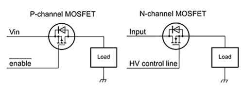 Figure 4: High-side load switches, positioned between the power source and the load, can be implemented with either P-channel or N-channel MOSFETs using appropriate gate-drive signals. (Image source: Nexperia)
If a P-channel MOSFET is used, pulling the gate low will turn the switch on and enable current flow into the load. The N-channel circuit requires a voltage higher than the input voltage to be applied in order to fully turn the MOSFET on. If a high-voltage signal is not available, a charge pump can be implemented to drive the N-channel gate. This adds to the complexity of the circuit, but since the N-channel MOSFETs have lower RDS(on) for a given size than a P-channel device, it may be worth the tradeoff. Another alternative would be to use the N-channel MOSFET as a low-side switch between the load and ground, reducing the required gate voltage.
Regardless of how the load switch is implemented, the voltage drop across the MOSFET is equal to the product of the drain current and RDS(on). The power loss is the product of the drain current squared and RDS(on). As such, a PMX100UNE operating at a maximum drain current of 0.7 A would have a power loss of only 58 mW due to its 120 mΩ channel resistance. This is why achieving the lowest possible value of RDS(on) is so important in the design of portable and wearable devices. Lower power loss means lower temperature rise and longer battery life.
MOSFET load switches can also be used to block reverse currents that may occur during a fault condition, such as a short circuit at the charging input. This is executed by placing two MOSFETs in series with reverse polarity (Figure 5).
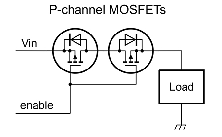 Figure 5: Shown is a reverse-current protected load switch using a common-drain circuit configuration and P-channel MOSFETs. (Image source: Nexperia)
Reverse-current protection in a load switch can also be implemented using a common source arrangement. This arrangement requires access to the common source point to effect a discharge of the gate after turn-on.
In-product applications
Good examples of up-and-coming wearable devices are AR and VR glasses. These devices need highly efficient components with low power dissipation and small physical size. They use a number of MOSFET devices as switches and in power conversion (Figure 6).
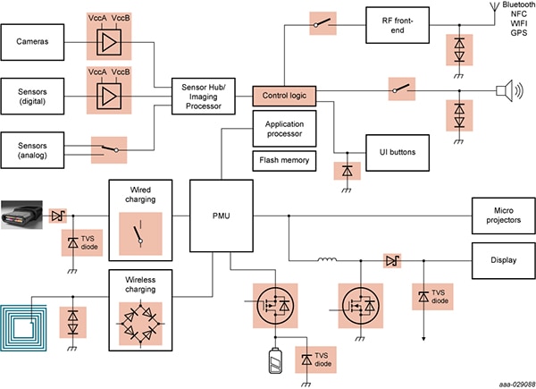 Figure 6: MOSFETs play critical roles in the design of AR/VR glasses as load switches, boost converters, and battery switches (marked within the orange squares). (Image source: Nexperia)
This type of wearable device has to balance extremely long recharge intervals with the “always-on” functionality expected by users. The MOSFET switches are used to power down sections of the device when they are not being used. Note the switches: these are implemented with MOSFETs that connect and disconnect the RF front-end and the loudspeaker. On the power control side, MOSFETs are used as a battery switch and to connect to an external power source for wired charging. They are also used in a switched-mode boost power converter for the display.
Conclusion
For designers of micro-wearables and other space and power-constrained devices, the Nexperia DFN0603 package MOSFETs offer the miniature package sizes best-in-class RDS(on) needed to implement next-generation designs. They are ideal components for use as load switches, battery switches, and in switched-mode power converters.

Disclaimer: The opinions, beliefs, and viewpoints expressed by the various authors and/or forum participants on this website do not necessarily reflect the opinions, beliefs, and viewpoints of DigiKey or official policies of DigiKey.


