How to Achieve Both DC Precision and Wide Bandwidth Using Zero-Drift Amplifiers
Contributed By DigiKey's North American Editors
2023-03-01
There are many real-world sensor signals, especially those related to natural phenomena, which exhibit only very slow and slight changes versus time. Yet it is these subtle changes that are important to developing insight and an understanding of the situation. Among the many examples are strain gages that monitor bridge or structure movement, underwater transducers for current flow, temperature-related phenomena, accelerometers sensing movement related to earthquakes and earth surface-plate shifts, outputs from various optical sensors, and nearly all biopotential signals.
Effectively and accurately capturing very low-level signals has always been a challenge. They are easily corrupted by noise, so amplifying them is critical to achieving the required amplitude and maintaining the signal-to-noise ratio (SNR). The low frequency of these signals, often in the single-digit or tens of hertz (Hz) and colloquially and universally referred to as “DC signals,” adds to the challenge.
Any initial DC offset in the amplifier’s parameters such as bias current or voltage offset, and inherent 1/f (pink) noise, as well as subsequent unavoidable performance shifts due to temperature-induced drift, power-rail variations, or component aging, will degrade the signal chain performance.
Traditionally, what are referred to as “zero-drift” amplifiers have been feasible only for lower bandwidth applications since dynamic error reduction techniques produce excessive artifacts at higher frequencies. However, that is a very limiting restriction, as these DC-like signals may have sudden bursts of important higher frequency, wider bandwidth activity, such as when a structure suddenly fractures or an earthquake occurs.
For this reason, a front-end amplifier that features very low drift for DC-like signals and has good higher frequency performance is very desirable. Fortunately, enhancements in topology and design have enabled development of zero-drift amplifier ICs for operation from DC to higher frequencies that essentially eliminate offset, parameter drift, and 1/f noise.
This article will use components from Analog Devices (ADI) to illustrate the specifics of zero-drift amplifiers, their parameters, and issues. It will then look at how the zero-drift amplifier functions are realized, as well as techniques to improve the performance of the amplifier and associated signal chain.
Dealing with non-zero drift
Drift is a shift in baseline performance and is due primarily, but not entirely, to various thermal effects in the sensor as well as the analog front-end (AFE) circuitry. The traditional solution to achieving near-zero drift is to use a chopper-stabilized amplifier which modulates the low-frequency signal (often called a DC signal) to a higher frequency that is easier to control and filter; subsequent output-stage demodulation by the amplifier restores the original signal, but in an amplified form. This technique works and has been successfully used for many years.
Note that “DC signal” is somewhat of a misnomer, and “near DC” would be more accurate. If the signal was truly DC and thus had a constant value, it would have no information-bearing variations – instead, it’s the slow variations that are of interest. Still, the common terminology is to use the term “DC signal.”
An alternative to chopper-based stabilization is the “auto-zeroing” approach. This technique uses dynamic correction to accomplish similar results, but with a somewhat different set of performance tradeoffs. Zero-drift operational amplifiers can use chopping, auto-zeroing, or a combination of both techniques to remove unwanted low-frequency error sources. Again, there is a minor terminology issue: the term “zero-drift” is slightly misleading: while these amplifiers do have extremely low, very close-to-zero drift, they are not perfect – even though they are impressively close. Each technique has its benefit and drawbacks and is used in different applications:
- Chopping uses signal modulation and demodulation and has lower baseband noise, but also produces noise artifacts at the chopping frequency and its harmonics.
- Alternatively, auto-zeroing uses a sample-and-hold circuit and is suitable for wider band applications, but has more in-band voltage noise due to noise “foldback” to the baseband part of the spectrum.
- Advanced zero-drift amplifier ICs combine both techniques to offer the best of both worlds. They manage the noise spectral density (NSD) to offer lower baseband noise while minimizing high-frequency errors such as ripple, glitches, and intermodulation distortion (IMD) (Figure 1).
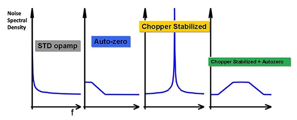 Figure 1: Each type of analog amplifier has a unique typical noise spectral density (NSD); the zero-drift amplifier accepts the NSD performance of the auto-zero and chopper-stabilized approaches to yield a more acceptable scenario. (Image source: Analog Devices)
Begin with chopping
The chopper-stabilized amplifier (also called a chopping amplifier or just a “chopper”) uses a chopping circuit to break up (chop) the input signal so that it can be processed as if it were a modulated AC signal. It then demodulates the signal back to a DC signal at the output to extract the original signal.
In this way, extremely small DC signals can be amplified while the effects of unwanted drifts are greatly minimized to near zero. The chopping modulation separates offset and low-frequency noise from the signal content by modulating the errors to higher frequencies, where they are much more easily minimized or removed via filtering.
Chopping operation details are easily understood in the time domain (Figure 2). The input signal (a) is modulated by the chopping signal (b) into a square wave. This signal is demodulated (c) at the output (d) back to DC. The inherent low-frequency errors (red waveform) in the amplifier are (c) modulated at the output to a square wave, which is then (d) filtered by a low-pass filter (LPF).
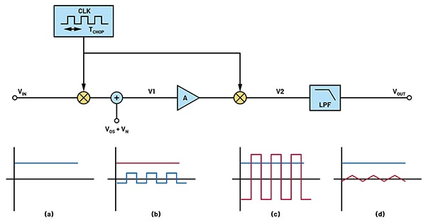 Figure 2: Time domain waveforms of the input signal VIN (blue) and errors (red) at (a) input, (b) V1, (c) V2, and (d) VOUT for the basic chopping technique. (Image source: Analog Devices)
Frequency-domain analysis is also instructive (Figure 3). The input signal (a) is modulated to the chopping frequency (b), processed by the gain stage at fCHOP, demodulated at the output back to DC (c), and finally passed through the LPF (d). The offset and noise sources (red signal) of the amplifier are processed at DC through the gain stage, modulated to fCHOP by the output chop switches (c), and finally filtered by the LPF (d). Since square-wave modulation is used, the modulation occurs around odd multiples of the modulation frequency.
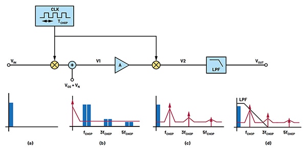 Figure 3: The spectrum in the frequency domain of the signal (blue) and errors (red) at (a) input, (b) V1, (c) V2, and (d) VOUT is also an important perspective. (Image source: Analog Devices)
Of course, no design is perfect. Both the time-domain and frequency-domain figures show that there will be some residual error due to the modulated noise and offset since the LPF is not a perfect “brick wall.”
Advance to auto-zeroing
Auto-zeroing is a dynamic correction technique that works by sampling and subtracting low-frequency error sources in an amplifier. A basic auto-zero amplifier consists of an amplifier with its unavoidable offset and noise, switches to reconfigure the input and output, and an auto-zero sampling capacitor (Figure 4).
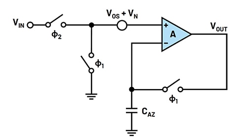 Figure 4: The basic auto-zero amplifier configuration shows the switches used to reconfigure the signal path and so capture the amplifier’s inherent errors on a capacitor. (Image source: Analog Devices)
During the auto-zero phase, ϕ1, the circuit’s input is shorted to a common voltage and the auto-zero capacitor samples the input offset voltage and noise. It is important to note that the amplifier is “unavailable” for signal amplification during this phase as it is occupied with another task. Thus, for an auto-zeroed amplifier to operate in a continuous manner, two identical channels must be interleaved in what is called “ping-pong” auto-zeroing.
During the amplification phase, ϕ2, the input is connected back to the signal path, and the amplifier is again available to amplify the signal. The low-frequency noise, offset, and drift are canceled by auto-zeroing. The remaining error is the difference between the current value and the previous sample of the errors.
Since low-frequency error sources do not change much from ϕ1 to ϕ2, this subtraction works well. However, the high-frequency noise is aliased down to baseband and results in an increased white-noise floor (Figure 5).
 Figure 5: The noise power spectral density is shaped by the chopping and auto-zero actions, as seen (left to right) before auto-zero, after auto-zero, after chop, and after chop and auto-zero. (Image source: Analog Devices)
The performance of advanced auto-zeroing IC amplifiers is impressive. They are typically better than even a “very good” precision op amp by one to two orders of magnitude in critical offset, drift, and noise specifications. So while their numbers are obviously not zero, they are very close to it.
For example, the ADA4528 is a single-channel, rail-to-rail (RTR), zero-drift amplifier that features a maximum offset voltage of 2.5 microvolts (μV), a maximum offset voltage drift of just 0.015 μV/°C, and a voltage noise density of 5.6 nano volts per root Hertz (nV)/√Hz) (at f = 1 kilohertz (kHz), gain of +100), and 97 nVpeak-peak (for f = 0.1 Hz to 10 Hz, gain of +100). The ADA4522, another single-channel RTR zero-drift amplifier, offers a maximum offset voltage of 5 μV, a maximum offset voltage drift of 22 nV/°C, a voltage noise density of 5.8 nV/√Hz (typical), and 117 nVpeak-peak from 0.1 Hz to 10 Hz (typical), along with an input bias current of 50 picoamps (pA) (typical).
Artifacts can diminish “perfection”
Although chopping works well to remove unwanted offset, drift, and 1/f noise, it inherently produces unwanted AC artifacts such as output ripple and glitches. However, due to careful examination of each artifact’s underlying cause, followed by the use of advanced or sophisticated topologies and process approaches, zero-drift products from Analog Devices have made the magnitude of these artifacts much smaller, and located them at higher frequencies where they are easier to filter out at the system level. These artifacts include:
Ripple: A basic consequence of the chopping modulation technique that moves these low-frequency errors to odd harmonics of the chopping frequency. Amplifier designers employ many methods to reduce the effects of ripple, including:
- Production offset trimming: The nominal offset can be significantly reduced by performing a one-time initial trim, but the offset drift and 1/f noise remain.
- Combining chopping and auto-zeroing: The amplifier is first auto-zeroed, then chopped to up-modulate the increased noise spectral density (NSD) to a higher frequency (as seen in the previous figure, which showed the resulting noise spectrum after chopping and auto-zeroing).
- Autocorrection feedback (ACFB): A local feedback loop can be used to sense the modulated ripple at the output and null out the low-frequency errors at their source.
Glitches: Transient spikes that are caused by charge injection mismatch from the chopping switches. The magnitude of these glitches depends on many factors, including source impedance and the amount of charge mismatch.
The glitch spikes not only cause artifacts at the even harmonics of the chop frequency, but also create a residual DC offset proportional to the chopping frequency. Figure 6 (left) illustrates what these spikes look like inside the chop switches at V1, and after the output chop switches at V2. Additional glitch artifacts at even harmonics of the chop frequency are caused by finite amplifier bandwidth (Figure 6, right).
 Figure 6: Glitch voltage (left) from charge injection at V1 (inside the chopping switches) and V2 (outside the chopping switches); glitches (right) caused by finite amplifier bandwidth at V1 and at V2. (Image source: Analog Devices)
Just as with ripple, amplifier designers have devised and implemented subtle but effective techniques to reduce the impact of glitches in zero-drift amplifiers.
- Charge injection trim: A trimmable charge can be injected into the inputs of a chopped amplifier to compensate for charge mismatch, which reduces the amount of input current at the op amp’s inputs.
- Multichannel chopping: This not only reduces glitch magnitude but also moves it to a higher frequency, making filtering easier. This technique results in more frequent glitches but with smaller magnitudes than simply chopping at a higher frequency.
A clear demonstration of multichannel chopping is seen in the comparison between a typical zero-drift amplifier (A) to the ADA4522, which uses this technique to significantly reduce the impact of glitches (Figure 7).
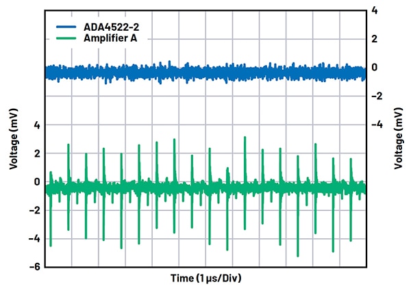 Figure 7: Due to its smaller noise glitches which are a result of its modified chopping technique, the ADA4522 reduces voltage spikes down to the noise floor. (Image source: Analog Devices)
From amplifier alone to system performance
Effective application of wideband zero-drift amplifiers requires careful consideration of system-level issues as well as the amplifier. Understanding where the remaining frequency artifacts are in the frequency spectrum, and their impact is critical.
The chopping frequency is usually but not always stated in the datasheet. It can also be determined by looking at the noise spectrum plot. For example, the datasheet of the ADA4528 explicitly states a chopping frequency of 200 kHz. It can also be seen in its noise density plot (Figure 8).
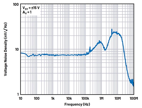 Figure 8: The stated ADA4528 datasheet chopping frequency specification of 200 kHz is reiterated by the noise density graph for the device. (Image source: Analog Devices)
The ADA4522 datasheet states that the chopping frequency is 4.8 megahertz (MHz) with an offset and ripple correction loop operating at 800 kHz. The noise density graph in Figure 9 shows these noise peaks. There is also a noise bump at 6 MHz due to the reduced phase margin of the loop when in unity gain, but this is not unique to zero-drift amplifiers.
 Figure 9: The graph of the noise density for the ADA4522 reveals not only the chopping frequency, but also other noise peaks due to various sources. (Image source: Analog Devices)
Designers should keep in mind that the frequency called out in the datasheet is a typical number and can vary from part to part. Therefore, a system design that requires two chopped amplifiers for multiple signal-conditioning channels should use a dual amplifier. This is because the two single amplifiers could have slightly different chopping frequencies, which in turn can interact and cause additional IMD.
Other system-level design conditions include:
- Matching input-source impedance: Transient current glitches interact with the input-source impedance to cause differential voltage errors, potentially resulting in additional artifacts at multiples of the chopping frequency. To minimize this potential source of error, each input of a chopped amplifier should be designed to see the same impedance.
- IMD and aliasing artifacts: A chopping amplifier input signal can mix with the chopping frequency, fCHOP, to create IMD at their sum and difference products, and their harmonics: fIN ± fCHOP, fIN ± 2fCHOP, 2fIN ± fCHOP, and so on. These IMD products can appear in the band of interest, especially as fIN approaches the chopping frequency. However, selecting a zero-drift amplifier with a chopping frequency that is much greater than the input-signal bandwidth greatly minimizes this issue by ensuring that likely “interferers” at frequencies which are close to fCHOP are filtered before this amplifier stage.
Chopping artifacts can also be aliased when sampling the amplifier output with an analog-to-digital converter (ADC). The specifics of these IMD products depend on glitch and ripple magnitudes and can vary from part to part, so it is often necessary to include antialiasing filters before the ADC to reduce this IMD.
Not surprisingly, filtering is critical to realizing the full potential of zero-drift amplifiers since it is the most-effective way to deal with these high-frequency artifacts at the system level. A low-pass filter between the zero-drift amplifier and the ADC reduces chopping artifacts and avoids aliasing.
Zero-drift amplifiers with higher chopping frequencies relax the requirements on the LPF and allow for wider signal bandwidth. Nonetheless, depending on how much out-of-band rejection is needed by the system and signal chain, a high-order active filter may be required rather than a simple one.
ADI has various resources to speed and simplify filter design, including a multiple feedback filter tutorial (MT-220) and the online Wizard filter design tool. Knowing the frequencies at which these chopping artifacts occur will help to create the required filter (Figure 10).
|
Figure 10: The table summarizes the types of noise and their spectral location for zero-drift amplifiers, and is a useful guide to assessing what kind of filtering is needed and where. (Image source: Analog Devices)
Getting that last bit of performance
One of the issues designers encounter when using superior components in conjunction with careful system design is that residual error sources now become significant. Error sources that were previously irrelevant or invisible now are limiting factors in achieving top-tier performance (it’s analogous to when a river dries up in a drought and new riverbed features are revealed for the first time). In other words, the third-order error sources become the issue when the first- and second-order error sources are minimized or eliminated.
For example, for zero-drift amplifiers and their analog signal channels, one potential source of offset error is the Seebeck voltage on the circuit board. This voltage occurs at the junction of two dissimilar metals and is a function of the temperature of the junction. The most common metallic junctions on a circuit board are solder-to-board trace and solder-to-component lead.
Consider the cross-section of a surface mount component soldered to a printed circuit board (pc board) (Figure 11). A variation in temperature across the board, such as with TA1 different than TA2, causes a mismatch in the Seebeck voltages at the solder joints, resulting in thermal voltage errors that degrade the ultralow offset voltage performance of the zero-drift amplifiers.
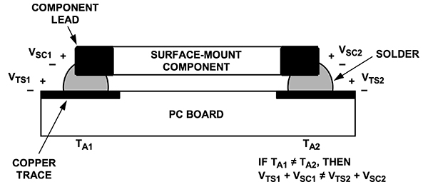 Figure 11: As advanced zero-drift amplifiers significantly reduce their errors, less-visible sources such as those due to thermal gradients and Seebeck voltage become the challenge and must be addressed. (Image source: Analog Devices)
To minimize these thermocouple effects, the resistors should be oriented so that the various heat sources warm both ends equally. Where possible, the input signal paths must contain matching numbers and types of components to match the number and type of thermocouple junctions. Dummy components, such as zero-ohm resistors, can be used to match the thermoelectric error source (with real resistors in the opposite input path). Placing matching components in close proximity, and orienting them in the same manner, will ensure equal Seebeck voltages, thus canceling thermal errors.
Additionally, it may be necessary to use leads of equal length to keep thermal conduction in equilibrium. The heat sources on the board should be kept as far away from the amplifier input circuitry as practical. Further, a ground plane can be used to help distribute heat throughout the board to maintain a constant temperature across the board and reduce EMI noise pickup.
Conclusion
Today’s zero-drift ICs offer highly stable and accurate performance, making them the solution to the challenge of AFEs in real-world applications requiring precision and consistency when capturing very low-frequency signals. They resolve the long-standing problem of accurately amplifying these signals that are at or near DC, as well as many situations where wider bandwidth is also required. By merging the two available techniques for building such amplifiers into a single IC – namely, chopper-based stabilization and auto-zeroing – designers benefit from the positive attributes of each approach, which also greatly minimizes their artifacts and shortcomings.

Disclaimer: The opinions, beliefs, and viewpoints expressed by the various authors and/or forum participants on this website do not necessarily reflect the opinions, beliefs, and viewpoints of DigiKey or official policies of DigiKey.


