Enhance SiC Device Efficiency Using Merged-Pin Schottky Diodes
Contributed By DigiKey's North American Editors
2025-03-12
Silicon carbide (SiC) has advantages over silicon (Si) that make it particularly suitable for Schottky diodes in applications such as fast battery chargers, photovoltaic (PV) battery converters, and traction inverters. Still, designers are being pushed to improve efficiency further.
Two ways to do this with SiC devices are to reduce leakage current and losses due to thermal resistance. While achieving these goals has been challenging, merged-pin Schottky (MPS) diodes offer a solution. MPS devices also enhance Schottky diode surge current performance.
This article explains the advantages of SiC Schottky diodes over conventional diodes for high-power applications, outlining where further performance enhancements can be achieved. It then introduces examples of MPS diodes from Nexperia, summarizes their key characteristics, and discusses how designers can benefit from their application.
The advantages of SiC Schottky diodes
The advantage of the SiC Schottky diode over a traditional Si P-N junction derives from the properties of the underlying semiconductor material and its design. SiC has a wider bandgap than Si. The bandgap is the energy needed to move electrons from the valence band to the conduction band in a semiconductor, and it is a crucial factor in determining the material's electrical conductivity.
SiC’s wider bandgap endows it with an order of magnitude higher dielectric breakdown field strength with a thinner drift layer for the same voltage rating when compared to an Si device. The drift layer is the lightly doped layer between a conventional diode's P and N layers, or the metal and P layers of a SiC Schottky diode. The thinner drift layer features lower resistivity and better electrical conduction performance from a smaller die size.
Another benefit of SiC is its approximately 3.5x better thermal conductivity, which improves power dissipation for a given chip area. The maximum operating temperature of SiC is nearly double that of Si. Utilizing a smaller die size decreases device self-capacitance, and the associated charges are lower for a specified current and voltage rating. These characteristics and SiC’s higher electron saturation velocity enable faster switching speeds with reduced losses.
From a construction perspective, instead of the conventional P-N junction, the Schottky diode dispenses with the P-type and instead uses a thin layer of metal (platinum, tungsten, gold, or another metal) bonded to N-type material. This bonding forms a metal-semiconductor (M-S) junction called a Schottky barrier (Figure 1).
 junction") Figure 1: Schottky diodes replace the P-type semiconductor of a conventional diode (top) with a metal to form an M-S junction (bottom). (Image source: DigiKey)
Figure 1: Schottky diodes replace the P-type semiconductor of a conventional diode (top) with a metal to form an M-S junction (bottom). (Image source: DigiKey)
The M-S junction generates a narrower electron depletion region in forward and reverse bias conditions than the P-N junction (Figure 2). The narrower depletion zone gives the Schottky diode a key advantage: a lower forward voltage (VF) than a conventional diode. When forward biased, the Schottky diode will typically start conduction at a few hundred millivolts compared with 0.6 to 0.7 volts for a P-N junction. This characteristic is advantageous for low-power applications such as battery-powered devices.
 Figure 2: The Schottky diode depletion zone is narrower in both forward and reverse bias conditions, resulting in a low forward voltage and reduced losses. (Image source: DigiKey)
Schottky devices conduct only through majority carriers (electrons), which results in negligible charge stored in the diode’s junction depletion layer when the component is forward biased. This limits losses (and power dissipation) when the diode switches from forward to reverse bias. In contrast, P-N junction diodes conduct through minority and majority carriers, which results in greater stored charges in the depletion layer. The outcome is higher switching losses for the P-N device, which multiply with increased frequency.
Overall, a Schottky diode will consume less power and tend to be more thermally efficient at dissipating heat in high-power applications than a P-N device. The reduction in dissipation enables the Schottky diode to withstand higher temperatures for more rugged performance and better reliability without the risk of thermal runaway.
A further advantage of the Schottky diode’s narrow depletion zone is that it endows the component with lower capacitance. Together with the SiC diodes’ “soft switching” behavior, this low capacitance significantly reduces electromagnetic interference (EMI).
How to make SiC Schottky diodes even better
SiC Schottky diodes continue to improve. For example, the narrow depletion zone of a contemporary SiC device multiplies the impact of the imperfections that occur when manufacturing the M-S interface, causing high leakage currents when the diode is reverse-biased. Moreover, the narrow depletion zone prevents the SiC Schottky diode from withstanding high reverse voltages (VR). A Schottky diode can withstand a VR of tens of volts, whereas a P-N junction can withstand hundreds of volts.
One solution to address the SiC diode’s high leakage currents is to thicken the diode’s drift layer and substrate. However, this increases electrical and thermal resistance, pushing up VF and junction temperature (TJ) for a given current. Moreover, the thickened drift layer’s higher resistance can impact surge current performance.
Nexperia has addressed this challenge with its MPS diode. The Nexperia PSC Series’ MPS structure uses two diode types, a SiC Schottky and a P-N device positioned in parallel. P-doped “wells” are implanted in the drift zone of a conventional Schottky device, forming a P-ohmic contact with the metal at the Schottky anode and a P-N junction with the lightly-doped SiC drift or epi-layer (Figure 3).
 Figure 3: The MPS structure uses two diode types, a SiC Schottky and a P-N device, positioned in parallel. P-doped areas are implanted in the drift zone to form a P-ohmic contact with the metal and a P-N junction with the SiC drift or epi-layer. (Image source: Nexperia)
Under reverse bias, the P-doped wells encourage the maximum field strength to move downwards into the almost defect-free drift layer, away from the metal barrier with its imperfections, reducing the overall leakage current (Figure 4).
 Figure 4: Adding P-doped wells to a SiC Schottky diode displaces the area of maximum field strength under reverse bias away from the anode metal. The result is lower leakage currents. (Image source: Nexperia)
The P-doped wells’ placement, area, and doping concentration affect the end characteristics and create a trade-off of VF drop against leakage and surge currents. The result is that an MPS device can operate at a higher breakdown voltage than a conventional SiC diode but with the same leakage current and drift layer thickness.
The hybrid combination of the Schottky diode (a unipolar device) and the P-N diode (bipolar) determines that the P-N junction does not conduct under normal conditions, and the effect is almost no reverse recovery losses. However, the hybrid arrangement improves surge current rating because the P-N diode conducts when transient overcurrent events occur, effectively protecting the hybrid component.
Because the MPS diodes behave like Schottky diodes under nominal conditions, the devices exhibit purely capacitive switching behavior, resulting in a lower reverse recovery charge (QRR) than an Si fast recovery diode with the same electrical rating. QRR, which is the stored charge in the diode that must recombine before the diode can block reverse voltage, is one of the main loss contributors of an Si diode.
Figure 5 compares the reverse recovery behavior of an Si diode compared to a SiC diode (Nexperia’s PSC1065HJ). The SiC diode exhibits purely capacitive switching, resulting in minimal QRR. The QRR is equivalent to the area of the graph under the IF = 0 axis.
 compared to a SiC diode (right) (click to enlarge)") Figure 5: Shown is the reverse recovery behavior of an Si diode (left) compared to a SiC diode (right). The SiC diode exhibits purely capacitive switching, resulting in minimal QRR. (Image source: Nexperia)
Figure 5: Shown is the reverse recovery behavior of an Si diode (left) compared to a SiC diode (right). The SiC diode exhibits purely capacitive switching, resulting in minimal QRR. (Image source: Nexperia)
Reducing drift layer thickness during manufacture
Because MPS diodes have significantly reduced leakage currents compared to conventional SiC diodes, an advantage can be gained from reducing the thickness of the drift layer. As noted above, for conventional SiC diodes, the drift layer is thicker than that used for Si diodes to keep leakage currents low.
During manufacture, the unprocessed SiC substrate is N-doped, and SiC epitaxial layers are ‘grown’ to form the drift region. The substrate can be up to 500 micrometers (µm) thick, which increases electrical and thermal resistance to the current and heat-flow path from the junction to the back-side metal. The result is an increased VF drop and TJ for a given current.
A solution to lower the electrical and thermal resistance of the drift layer is to reduce the thickness of the underside of the substrate by grinding during the manufacturing process (Figure 6). The result is an MPS diode, which, for given operating conditions, will display a lower operating temperature, higher reliability, higher surge current capability, and lower VF drop than a comparable SiC diode.
 Figure 6: Reducing the thickness of the underside of the substrate (right) results in an MPS diode, which will display a lower operating temperature, higher reliability, higher surge current capability, and lower VF drop than a comparable SiC diode. (Image source: Nexperia)
Commercial options
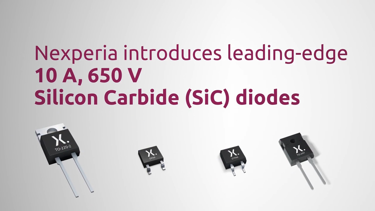
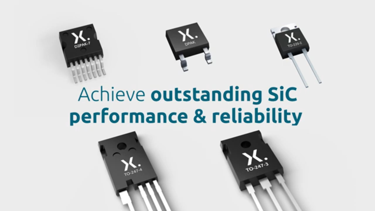
Nexperia offers a range of MPS diodes for applications as diverse as battery charging infrastructure, server and telecom power supplies, uninterruptible power supplies, and PV inverters.
The PSC0665HJ (Figure 7) is an MPS SiC Schottky diode encapsulated in a DPAK R2P (TO-252-2) surface mount package. The thermal resistance from junction to case (Rth(j-c)) is 2.7 Kelvin/watt (K/W). Total power dissipation (Ptot) (Tc ≤ +25°C) is 115 W. The diode offers temperature-independent capacitive turn-off and zero recovery switching behavior combined with a good figure-of-merit (FOM) (FOM = total capacitive charge (QC) x VF). The component offers solid surge current protection, indicated by a high non-repetitive peak forward current (IFSM).
 Figure 7: The PSC0665HJ is an MPS SiC Schottky diode encapsulated in a DPAK R2P (TO-252-2). (Image source: Nexperia)
QC for the PSC0665HJ is 14 nanocoulombs (nC) (at a VR = 400 V; dIF/dt = 200 A/microsecond (A/µs); forward current (IF) ≤ 6 A; TJ = +25°C) and VF = 1.5 V (at IF = 6 A; TJ = +25°C). That gives an FOM for the diode of 14 nC x 1.5 V = 21 nanojoules (nJ).
The maximum repetitive peak reverse voltage (VRRM) is 650 V. Reverse current (IR) is 1 µA at +25°C, with a VR of 650 V. Maximum forward current (IF) is 6 A, and maximum IFSM is 300 A (tp = 10 µs; square wave; Tc = +25°C) or 36 A (tp = 10 ms; half sinewave; Tc = +25°C).
The PSC2065LQ is another offering in the Nexperia MPS SiC Schottky diode family. This device comes encapsulated in a TO247 R2P (TO-247-2) through-hole power plastic package. The thermal resistance from junction to case (Rth(j-c)) is 1 W. Ptot (Tc ≤ +25°C) is 115 W.
QC for the PSC2065LQ is 41 nC (at a VR = 400 V; dIF/dt = 200 A/µs; IF ≤ 20 A; Tj = +25°C) and VF = 1.5 V (at an IF = 20 A; TJ = +25°C). That gives an FOM of 41 nC x 1.5 V = 61.5 nJ.
VRRM is 650 V. IR is 1 µA at +25°C, at a VR of 650 V. Maximum IF is 10 A and maximum IFSM is 440 A (tp = 10 µs; square wave; Tc = +25°C) or 52 A (tp = 10 ms; half sinewave; Tc = +25°C).
Conclusion
Compared to Si, SiC Schottky diodes provide superior technical advantages, such as significantly better switching performance and higher switching frequencies, without sacrificing output power or overall system efficiency. More performance gains for SiC Schottky diodes have been achieved with the hybrid MPS construction from Nexperia that takes advantage of a SiC Schottky diode in parallel with a P-N diode. The result is a device that, for given operating conditions, will display a lower operating temperature, higher reliability, higher surge current capability, and lower VF drop than a comparable SiC diode.
Disclaimer: The opinions, beliefs, and viewpoints expressed by the various authors and/or forum participants on this website do not necessarily reflect the opinions, beliefs, and viewpoints of DigiKey or official policies of DigiKey.