Design a Simple and Compact UPS Based on a Supercapacitor
Contributed By DigiKey's North American Editors
2024-03-15
An uninterruptible power supply (UPS) is vital for applications such as data protection in redundant array of independent disks (RAID) storage, automotive telemetry for safety operations, and medication delivery devices such as insulin pumps in healthcare.
However, designing a UPS can be challenging, especially if space is limited. Moreover, careful design is required for the many applications that cannot tolerate energy flows from the storage system back to the power supply.
These design challenges can be eased by considering an integrated approach whereby multiple converters and charging circuits are replaced with a single component. This integrated approach simplifies circuit design and makes it easier to ensure that no current flows back to the power supply during backup operation.
This article outlines UPS design challenges and presents a conventional solution. The article then introduces a simplified, integrated alternative based on a buck/boost switching regulator from Analog Devices.
Using a supercapacitor as an energy reservoir
Figure 1 shows a conventional approach to a UPS design. The UPS powers a 24 volt DC (VDC) sensor in this example. The sensor circuit requires a 3.3 and a 5 volt input. The UPS uses a linear regulator to charge a supercapacitor when system voltage is available. If the system voltage drops, the energy in the capacitor is boosted to the required supply voltage level with a step-up regulator.
 Figure 1: This UPS charges a supercapacitor while the system voltage is normal and draws on that energy when the system voltage drops. (Image source: Analog Devices)
If the 24 volt supply is also used to power other circuit elements beyond the sensors, the supercapacitor should be incorporated such that it only powers the sensor circuit and not the other electronics associated with the 24 volt line. Diode “D” prevents this from happening when the circuit is in backup mode.
This system works well but can be difficult to implement because it uses several voltage converters. It can also be challenging if space is limited. Figure 2 illustrates an alternative approach. This approach uses a single backup regulator to replace the multiple regulators in the circuit shown in Figure 1, saving space and simplifying the design.
 Figure 2: An integrated backup regulator makes UPS designs more straightforward and compact. (Image source: Analog Devices)
An integrated backup solution
The design concept illustrated in Figure 2 can be realized using Analog Devices’ MAX38889 buck/boost switching regulator. This is a flexible and compact storage capacitor or capacitor bank backup regulator for transferring power efficiently between a storage element and a system supply rail. It measures 3 x 3 millimeters (mm) and outputs 2.5 to 5.5 volts (VSYS) at a maximum current of 3 amperes (A) (ISYSMAX) from a supercapacitor input (VCAP) of 0.5 to 5.5 volts (Figure 3). The regulator’s operating temperature range is -40°C to +125°C.
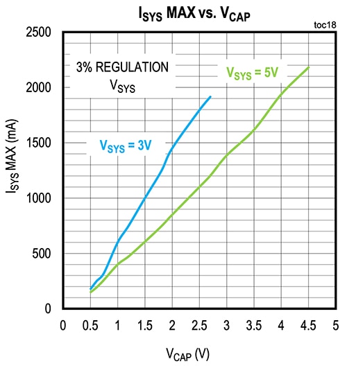 Figure 3: For a UPS based on the MAX38889, the ISYSMAX for a given VSYS depends upon VCAP. (Image source: Analog Devices)
When the main power supply is present, and its voltage is above the minimum threshold system supply voltage, the regulator charges the supercapacitor with a maximum 3 A peak and 1.5 A average inductor current. Once the supercapacitor is fully charged, it draws just 4 microamperes (µA) quiescent current while maintaining a ready state. The supercapacitor must be fully charged to enable backup operation.
When the main supply is removed and the supercapacitor is fully charged, the regulator prevents the system from dropping below the set system backup operating voltage (VBACKUP). It does this by boosting the supercapacitor discharge voltage to VSYS, the regulated system voltage. During backup operation, the MAX38889 uses an adaptive, on-time, and current-limited pulse frequency modulation (PFM) control scheme.
The external pins of the regulator allow control of various settings, such as maximum supercapacitor voltage (VCAPMAX), VSYS, and peak inductor charge and discharge current.
The MAX38889 implements a True Shutdown feature, disconnecting SYS from CAP and protecting against a SYS short if VCAP > VSYS. Charging and backup can be disabled by keeping the ENC and ENB pins low, respectively (Figure 4).
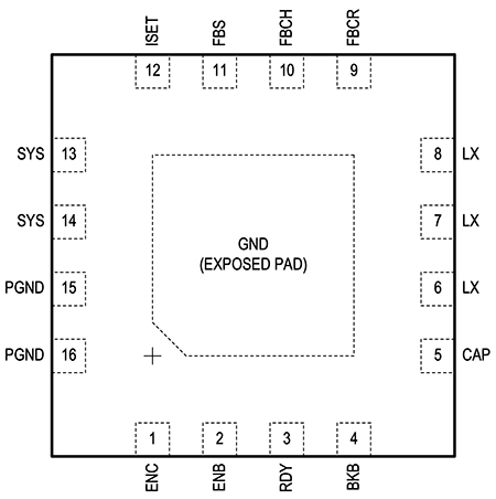 Figure 4: The external pins of the MAX38889 allow settings of maximum supercapacitor voltage VCAPMAX, VSYS, and peak inductor charge and discharge current; the backup system status can be monitored through the RDY flag. (Image source: Analog Devices)
The backup system status can be monitored through two status outputs: the ready status (RDY) flag, which indicates when the supercapacitor is charged, and the backup status (BKB) flag, which indicates backup operation.
Supercapacitor selection
Figure 5 shows a simplified application circuit for the UPS based on the MAX38889. VCAPMAX during charging is determined by the resistor-divider driving the FBCH pin. In this example, the resistor values of R1 = 1.82 megaohms (MΩ), R2 = 402 kilohms (kΩ), and R3 = 499 kΩ ensure the VCAPMAX is set to 2.7 volts. The supercapacitor is charged with a maximum 3 A peak and 1.5 A average inductor current. During discharge, the peak inductor current is 3 A.
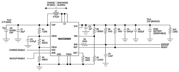 Figure 5: Shown is a simplified application circuit for a UPS based on the MAX38889. The supercapacitor is charged with a maximum 3 A peak and 1.5 A average inductor current. During discharge, the peak inductor current is 3 A. (Image source: Analog Devices)
Care is required when selecting the supercapacitor for backup operation. When the main power source fails, load power is provided by the MAX38889 operating in backup or boost mode using the supercapacitor as the energy source. The power the supercapacitor can deliver at its minimum regulation supply voltage must be greater than the system requires.
The MAX38889 presents a constant power load to the supercapacitor, causing less current to be drawn from it when it operates near VCAPMAX. However, the current drawn from the supercapacitor increases as it discharges (and the voltage drops) to maintain constant power to the load. The energy required in backup mode is the product of the continuous backup power (VSYS x ISYS) over the duration of backup operation (TBACKUP).
The amount of energy in joules (J) available in the supercapacitor (CSC) is calculated using Equation 1:
 Equation 1
The amount of energy required to complete the backup operation is calculated using Equation 2:
 Equation 2
Where ISYS is the load current during backup.
Since the energy required for the load during the backup event is supplied by the supercapacitor, assuming a conversion efficiency (η) and given a required TBACKUP, the required CSC value in farads (F) is determined using Equation 3:
![CSC = 2 x VSYS x ISYS x TBACKUP / [(V2CAPMAX - V2CAPMIN) x η] Equation 3](http://sc-c.digikeyassets.com/-/media/Images/Article%20Library/TechZone%20Articles/2024/March/Design%20a%20Simple%20and%20Compact%20UPS%20Based%20on%20a%20Supercapacitor/article-2024march-design-a-simple-and-compact-equation3.jpg?la=en&ts=56f7047a-89d0-47e4-bd11-713261dba04e) Equation 3
Equation 3
Using the application circuit shown in Figure 5 as an example, assuming a 200 milliampere (mA) system load, an average efficiency of 93%, and a backup time of 10 seconds (s), the minimum value of the supercapacitor required is:
![CSC = 2 x 3,0 V x 10s / [((2.7 V)2 - (1.5 V)2) x 0.93] = 2.56F Equation 4](http://sc-c.digikeyassets.com/-/media/Images/Article%20Library/TechZone%20Articles/2024/March/Design%20a%20Simple%20and%20Compact%20UPS%20Based%20on%20a%20Supercapacitor/article-2024march-design-a-simple-and-compact-equation4.jpg?la=en&ts=be3fec53-026f-41b8-b814-0535a2a69936) Equation 4
Equation 4
Figure 6 shows the charge and discharge curves for the application circuit shown in Figure 5.
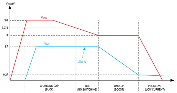 Figure 6: Charge and discharge curves for the application circuit shown in Figure 5. VSYS = 3.6 volts, VCAP = 2.7 volts, VBACKUP = 3 volts. (Image source: Analog Devices)
Get started with an evaluation board
The MAX38889AEVKIT# Capacitor Charger Power Management Evaluation Board provides a flexible circuit to evaluate the buck/boost backup regulator and test a UPS based on the MAX38889 and a supercapacitor. External components allow for a wide range of system and supercapacitor voltages, as well as charging and discharging currents.
The board incorporates three shunts: ENC (charging enabled), ENB (backup enabled), and LOAD (Figure 7). With the ENC shunt set in position 1-2, charging is enabled when VSYS is above the charging threshold. With the ENB shunt set in position 1-2, backup is enabled when VSYS drops below the backup threshold. The LOAD shunt can be set to position 1-2 to enter a test mode whereby a 4.02 ohm (Ω) load is connected across VSYS and ground to simulate a discharging scenario. The board enters normal operating mode if the shunt is only connected to one pin.
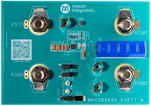 Figure 7: The MAX38889AEVKIT provides a flexible circuit to evaluate the MAX38889 buck/boost supercapacitor backup regulator. (Image source: Analog Devices)
When the main battery provides more than the minimum system voltage required for charging, the MAX38889 regulator charges the supercapacitor with an average current of 1.5 A. with VFBCH = 0.5 volts and with resistors R1 = 499 kΩ, R2 = 402 kΩ, and R3 = 1.82 MΩ, then VCAPMAX = 2.7 volts.
The EVKIT VBACKUP is set to 3 volts by resistors R5 (1.21 MΩ) and R6 (1.82 MΩ) with VFBS = 1.2 volts. This dictates that when the main battery is removed and VFBS drops to 1.2 volts, the MAX38889 draws power from the supercapacitor and regulates the VSYS to VBACKUP.
The MAX38889A EVKIT provides a RDY test point to monitor the supercapacitor charge status. The RDY test point is high when the voltage of the FBCR pin crosses the FBCR voltage threshold of 0.5 volts (set by R1, R2, and R3). This means the RDY goes high when the VCAP exceeds 1.5 volts. Similarly, when the supercapacitor provides backup, the RDY flag goes low when the supercapacitor provides less than 1.5 volts.
The EVKIT also provides a BKB test point to monitor the system backup status. The BKB is pulled low when the system provides backup power, and pulled high when the system is charging or in an idle state.
A resistor (R4) sets the peak inductor current between ISET and ground (GND). A resistor value of 33 kΩ sets the peak inductor current to 3 A according to the formula: Peak charging current (ILX_CHG) = 3 A x (33 kΩ/R4) (Figure 8).
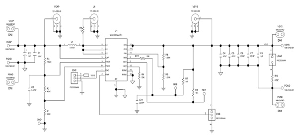 Figure 8: Shown is a schematic of the MAX38889 evaluation board; it operates using an 11 F supercapacitor and provides test points to monitor VCAP, VSYS, RDY, and BKB. (Image source: Analog Devices)
Conclusion
A supercapacitor can be used as the energy storage element for a UPS. Conventional UPS topologies use multiple voltage regulators that take significant space, making them tricky to design. An integrated buck/boost regulator approach eases these design challenges by replacing multiple converters and charging circuits with a single compact component.

Disclaimer: The opinions, beliefs, and viewpoints expressed by the various authors and/or forum participants on this website do not necessarily reflect the opinions, beliefs, and viewpoints of DigiKey or official policies of DigiKey.


