ADI's Data Acquisition Solution Shines in Advanced Lithography Chip Manufacturing
Contributed By DigiKey's North American Editors
2025-02-13
The semiconductor manufacturing equipment (SME) market is projected to experience substantial growth over the next five years, driven by the anticipated increase in semiconductor chip sales from $600 billion in 2022 to $1 trillion in 2030. Sensors are at the heart of the advanced lithography systems used in chip manufacturing.
Manufacturing the complex, high-performance—and ever smaller—semiconductor chips is largely reliant on highly precise and sensitive lithography processes that are instrumental in printing intricate patterns onto silicon wafers and other substrates used in chip manufacturing.
Advanced lithography systems employ extremely accurate and sensitive techniques, which not only enhance process yield but also minimize waste and optimize plant efficiency. To achieve the sub-micron and nanometer precision essential for mass producing integrated circuits (ICs), these systems rely on thousands of sensors for monitoring and controlling position, temperature, energy, and motion.
Overall system performance relies on the precise and repeatable performance of each individual sensor. Advanced algorithms interpret large volumes of sensor data and coordinate the necessary tweaks in very minor but detailed ways using thousands of actuators.
Analog Devices, Inc. (ADI) leverages its signal chain micromodule (µModule®) technology to provide a high-performance, miniaturized, analog-to-digital data acquisition (DAQ) solution for monitoring and controlling lithography semiconductor manufacturing subsystems to meet the production challenges faced by wafer fabricators and integrated device manufacturers.
Application background
The continued miniaturization of semiconductors is driving performance gains in everything from smartphones to supercomputers, and the processing requirements of generative artificial intelligence (GenAI), quantum computing, IoT, and edge computing. Advanced processes and innovative control systems are required to meet the ever-decreasing size requirements of semiconductors with circuits as narrow as one-ten-thousandth the width of a human hair.
Lithography is a cornerstone technology in semiconductor manufacturing that enables the precise patterning of features on silicon and other substrate wafers to create ICs. It utilizes photomasks and powerful, extremely accurate light beams or radiation to transfer the details of a chip's design pattern onto wafers, which are coated with photoresist material. The photoresist reacts to the light, and the wafer is treated with chemicals to etch the circuit pathways in the wafer substrate. Multiple photomasks are utilized in a layering process.
The highly specialized and extremely complex lithography semiconductor manufacturing systems are produced by a very small number of companies able to undertake the technical challenges and fund the expensive R&D needed for continued innovation in this field.
ASML is the industry leader, dominating the advanced lithography market with its exclusive, cutting-edge extreme ultraviolet (EUV) systems, which are essential for producing the most advanced chips. Costing up to hundreds of millions of dollars, the company's most advanced systems now enable the production of chips with feature sizes smaller than 2 nm, providing more transistors per chip and smaller spacing between transistors. It also supplies deep ultraviolet (DUV) systems that utilize longer wavelengths suitable for more cost-effective production of mid-range and legacy layers on chips manufactured at 14 nm, 28 nm, and larger nodes.
Other lithography semiconductor manufacturing systems are produced by Canon and Nikon, which focus on DUV lithography and legacy technologies for manufacturing less advanced nodes used in MEMS, power semiconductors, and industrial applications.
Achieving extreme precision
Lithography processes require extreme precision to achieve sub-micron scale patterns. Sensors and actuators are critical to maintain precision and yield, enabling continued technological advances in the development of smaller, more potent, and energy-efficient semiconductors.
Sensors play a pivotal role in actuator control, providing real-time feedback, error correction, and environmental compensation:
- Position sensors measure the exact position of wafers, photomasks, and lenses
- Vibration sensors detect and compensate for vibrations that can disturb alignment
- Environmental sensors monitor temperature, humidity, and air quality to minimize environmental influences on precision
- Force and strain sensors ensure actuators apply the correct forces during alignment and positioning
Sensors provide the essential real-time data for closed-loop feedback to adjust actuators dynamically, ensuring alignment and pattern accuracy. They detect deviations in real time to prevent defects in patterned wafers and perfect alignment of the photomask and wafer, which is crucial for multi-layer chip designs. They are also critical for minimizing delays caused by misalignments or rework.
Interaction of sensors and actuators
DUV and EUV lithography systems both rely on tens of thousands of sensors to achieve the precision and reliability essential for efficient, high-yield semiconductor manufacturing. As equipment manufacturers aim to achieve picometer scale for next-generation lithography, the role of sensors and actuators in ensuring precision and reliability becomes ever more critical. The seamless interaction and management of those components are central to the success of lithography systems.
Managing these sensors requires real-time data processing and advanced control systems. Interaction between sensors and actuators in lithography systems must be meticulously orchestrated to attain the precision and reliability demanded by semiconductor manufacturers and their customers. The intricate processes hinge on real-time feedback mechanisms, sophisticated control algorithms, and seamless integration across intricate subsystems.
Sensors continuously monitor parameters such as position, temperature, pressure, and vibration. Any deviation from desired parameters must be corrected in real time. Actuators are directed to respond with micro or nano-scale adjustments to position the wafer or mask, and fine-tune the optical focus or light source alignment.
In wafer stage positioning, sensors track movements with sub-nanometer precision. Actuators, such as linear motors or piezoelectric elements, dynamically adjust the stage’s position to maintain accurate alignment with the photomask. Optical alignment sensors monitor the light path, and actuators adjust mirrors or lenses to ensure focus and pattern accuracy.
Centralized control
Centralized control units monitor and process data from thousands of sensors and send commands to actuators. These systems utilize high-speed processors and sophisticated algorithms to manage interactions seamlessly, ensuring synchronization across multiple subsystems. Achieving nanometer-level accuracy requires minimal delays in data processing and actuator response.
Sensors and actuators are connected via high-speed, low-latency communication protocols like EtherCAT, Ethernet, or proprietary interfaces. These networks facilitate rapid data exchange and coordination between components.
Drift in sensor readings or actuator performance is detected through monitoring and compensated using adaptive control algorithms. Machine learning algorithms analyze historical data to predict potential deviations or equipment wear, enabling predictive maintenance and optimized actuator performance.
As semiconductor nodes continue to shrink, the role of sensor and actuator integration is increasingly critical. Interferometers measure the wafer stage position with nanometer precision, while actuators dynamically adjust the stage position based on feedback from alignment and vibration sensors. Optical sensors monitor light focus and intensity, and piezoelectric actuators adjust lenses or mirrors to maintain focus for accurate projection of circuit designs onto the wafer. Cameras or optical sensors are also utilized to detect particles or irregularities, with actuators being prompted to reposition the wafer or mask to avoid defects, or initiate automated cleaning procedures.
Signal chain performance
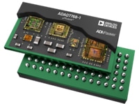
In each lithography semiconductor manufacturing system, the performance of each sensor is critical. ADI's ADAQ7768-1 (Figure 1) is a DAQ system based on the company's µModule technologies that is designed to simplify and enhance the performance of precision measurement and control systems. The single system-in-package (SiP) solution incorporates high input impedance amplification, anti-aliasing, signal conditioning, analog-to-digital (A/D) conversion, and configurable digital filtering blocks.
 Figure 1: ADI's ADAQ7768-1 µModule data acquisition system. (Image source: Analog Devices, Inc.)
By integrating passive components such as resistors and capacitors and active components such as op-amps, references, low dropout regulators (LDOs), and A/D conversion, μModules guarantee the performance of a complete signal chain over temperature and power supply variations. This ensures precise and repeatable high-performance signal chains for acquiring signals from pressure, temperature, and vibration sensors.
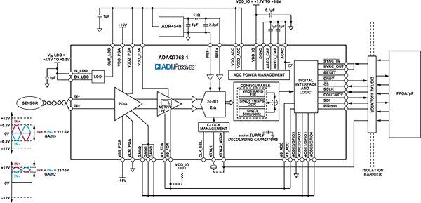
The ADAQ7768-1 integrates multiple components into a single µModule, as shown in the Figure 2 block diagram. These include a 24-bit precision analog-to-digital converter (ADC), signal conditioning components such as amplifiers and filters, and power management and reference circuitry.
 Figure 2: A block diagram of the ADAQ7768-1 µModule. (Image source: Analog Devices, Inc.)
The 24-bit ADC enables precise measurements of delicate parameters such as vibration levels in wafer stages, thermal variations in optical assemblies, and sub-nanometer positioning errors.
Multiple sensors—such as pressure, temperature, and vibration—can be wired to the ADAQ7768-1's analog front end (AFE), which includes multiple active and passive components. Multiple modules can be used in parallel to manage data from a large array of sensors, such as those monitoring wafer stage alignment or environmental conditions.
Power supply noise can directly impact the precision and reliability of lithography system measurements, but the ADAQ7768-1 was designed to operate with a single power supply, simplifying system design and reducing the need for additional external power management circuits.
The power management design minimizes power supply ripple and noise, which is critical for maintaining the high accuracy of the integrated low noise 24-bit ADC and the signal conditioning chain.
The ADAQ7768-1 is designed to operate using a single regulated 5.3 V input, with minor variation of input voltage range between 5.1 V and 5.5 V. The module includes internal LDOs to provide clean and stable power to its various internal subsystems.
The ADAQ7768-1 reduces design complexity by eliminating the need for designers to source and calibrate individual signal chain components, helping to streamline prototyping and testing phases, thereby shortening the time-to-market.
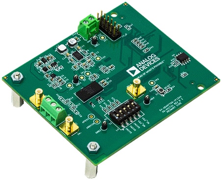
Product designers can utilize ADI's EVAL-ADAQ7768-1 evaluation board (Figure 3) to simplify prototyping, accelerate development, and help validate precision data acquisition designs that integrate the ADAQ7768-1 into their systems. This is critical in ensuring systems perform as expected in sub-nanometer positioning and alignment processes.
 Figure 3: ADI's evaluation board for prototyping and testing applications built around the ADAQ7768-1 data acquisition solution. (Image source: Analog Devices, Inc.)
The evaluation board provides a fully functional platform to test the ADAQ7768-1 with pre-assembled signal chain components and offers plug-and-play operation with standard test equipment or microcontrollers. Designers can evaluate and optimize the performance of their designs, test under various environmental conditions test differing sensor types and signal sources to determine optimal input signal conditioning.
Conclusion
Advanced lithography systems, which rely on thousands of sensors for monitoring and control, are crucial for manufacturing smaller and more powerful semiconductors. Sensors play a pivotal role in actuator control, providing real-time feedback and ensuring precision and yield in semiconductor manufacturing. ADI’s ADAQ7768-1 data acquisition system simplifies and enhances precision measurement and control systems, integrating signal conditioning, conversion, and processing blocks. Its compact size, high accuracy, and ease of use make it a valuable tool for developing next-generation lithography equipment that demands extreme precision and reliability.

Disclaimer: The opinions, beliefs, and viewpoints expressed by the various authors and/or forum participants on this website do not necessarily reflect the opinions, beliefs, and viewpoints of DigiKey or official policies of DigiKey.


