

Presented By

PCB Trace Width Calculator
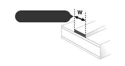
This tool uses formulas from IPC-2221 to calculate the width of a copper printed circuit board conductor or "trace" required to carry a given current while keeping the resulting increase in trace temperature below a specified limit. If the length of the trace is also provided, the total resistance, voltage drop, and power loss due to trace resistance are also calculated. The results are estimates; actual results may vary depending on application conditions. Note also that required widths are significantly higher for traces on internal layers of a circuit board compared to those on a board’s outer surface; use whichever result is appropriate for your situation.
Formula
First, calculate the Area:
Then, calculate the Width:
For IPC-2221 internal layers: k = 0.024, b = 0.44, c = 0.725
For IPC-2221 external layers: k = 0.048, b = 0.44, c = 0.725
Where k, b, and c are constants resulting from curve fitting to the IPC-2221 curves.
Common values:
Thickness: 1 oz
Ambient: 25 C
Temp rise: 10 C
Minimum Trace Width

Internal Layers
Minimum Trace Width
External Layers in Air


Recommended Products
Samtec Inc Related Articles
Presented By

