PCIe® Clock Buffers and Generators
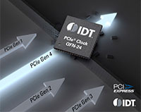
Renesas offers PCIe Gen1-4 clock generation for riser cards, storage, networking, JBOD, communications, and access points with its 9DBL0x and 9FGL0x devices
 Renesas’ 9DBL0x PCIe clock buffer devices are 3.3 V members of Renesas’ full-featured PCIe family. The 9DBL0x support PCIe Gen1-4 common clocked (CC) and PCIe separate reference independent spread (SRIS) systems. They offer a choice of integrated output terminations providing direct connection to 85 Ω or 100 Ω transmission lines.
Renesas’ 9FGL0x PCIe clock generator devices are also, 3.3 V members of Renesas’ 3.3 V full-featured PCIe family. The devices have 2-, 4-, 6-, and 8-output enables for clock management and support two different spread spectrum levels in addition to spread off. The 9FGL0x supports PCIe Gen1-4 common clocked architectures (CC) and PCIe separate reference no-spread (SRnS) and separate reference independent spread (SRIS) clocking architectures.
The 9DBL0xP1 and 9FGL0xP1 devices can be factory programmed with a user-defined power up default SMBus configuration.
- PCIe Gen1-2-3-4 CC compliant in ZDB mode
- PCIe Gen2 SRIS compliant in ZDB mode
- Supports PCIe Gen2-3 SRIS in fan-out mode
- Supports PCIe SRnS clocking
- Direct connection to 100 Ω (xx42) or 85 Ω (xx52) transmission lines
- Saves 8, 16, 24, or 32 resistors compared to standard PCIe devices
- Spread spectrum tolerant; allows reduction of EMI
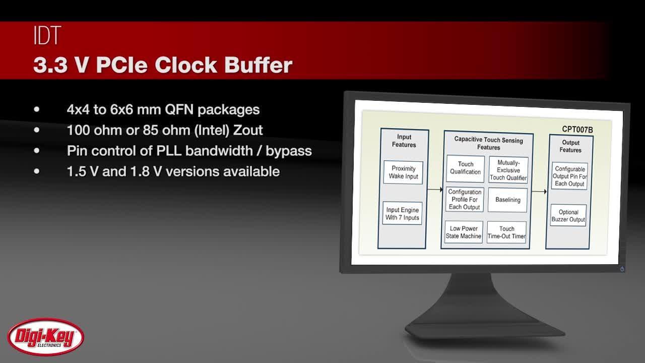
- Pin/SMBus selectable PLL bandwidth and PLL Bypass
- Minimizes phase jitter for each application
- Device contains default configuration
- SMBus interface not required for device operation.
- Easy AC-coupling to other logic families
- See Renesas application note AN-891
- Space-saving 24-pin 4 mm x 4 mm (9DBL02), 32-pin 5 mm x 5 mm (9DBL04), 32-pin 5 mm x 5 mm (9DBL06), or 48-pin 6 mm x 6 mm (9DBL08) VFQFPN; minimal board space
- PCIe Gen1-2-3-4 CC-compliant
- PCIe Gen2-3 SRIS-compliant
- Direct connection to 100 Ω (xx41) or 85 Ω (xx51) transmission lines
- Saves 8, 16, 24, or 32 resistors compared to standard PCIe devices
- Pin/SMBus selectable 0%, -0.25%, or -0.5% spread on DIF outputs
- Minimizes EMI and phase jitter for each application
- Supports PCIe SRnS clocking
- One 3.3 V LVCMOS REF output with Wake-On-LAN (WOL)support
- Easy AC-coupling to other logic families
- See Renesas application note AN-891
- Space saving 24-pin 4 mm x 4 mm (9FGL02), 32-pin 5 mm x 5 mm (9FGL04), 40-pin 5 mm x 5 mm (9FGL06), or 48-pin 6 mm x 6 mm (9FGL08) VFQFPN; minimal board space
9DBL0x PCIe Zero-Delay Buffers
| Image | Manufacturer Part Number | Description | Available Quantity | Price | View Details | |
|---|---|---|---|---|---|---|
 |  | 9DBL0242BKILF | IC CLK FANOUT/BUFF ZD 24VFQFPN | 364 - Immediate | $24.63 | View Details |
 |  | 9DBL0442BKILF | IC CLK FANOUT/BUFF ZD 32VFQFPN | 0 - Immediate | See Page for Pricing | View Details |
 |  | 9DBL0641BKILF | IC CLK FANOUT/BUFF ZD 40VFQFPN | 0 - Immediate | See Page for Pricing | View Details |
 |  | 9DBL0841BKILF | IC CLK FANOUT/BUFF ZD 48VFQFPN | 0 - Immediate | See Page for Pricing | View Details |


