Reimagining Point-of-Load Power Conversion
Ask any system architect: “What is your biggest problem?” The likely answer is that the devices powering the system occupy between 30–50% of the board space, not to mention the added filtering and electromagnetic interference (EMI) suppression components required. In most electronic systems—from consumer applications to datacenter and networking products—power remains one of the major constraints to size and height reduction.
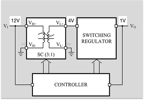
 Figure 1. Murata’s two-stage buck architecture includes a charge pump followed by a buck switching regulator. (Image source: Murata)
Traditionally, system architects have depended on buck point-of-load (POL) converters to step down current from bus rails, such as 12 V, to power system loads, such as core and application processors, system ASICs, and memory. Buck conversion has served the industry well for several decades and has been refined and improved to form robust and cost-effective solutions. However, to make real strides in power density, system architects need to think beyond just iterative improvements. For this reason, Murata has introduced a two-stage POL converter which consists of a charge pump followed by a buck switching regulator, as shown in Figure 1.
For many, the idea of a two-stage architecture providing efficiency improvement may seem counterintuitive as the efficiency of the individual stages are multiplied together. However, due to innovative switched-capacitor techniques, the charge pump is virtually lossless, leading to exceptional efficiency on the first conversion stage.
Considering the typical example of 12 Vin to 1 Vout as shown in Figure 1, the charge pump is using capacitors to divide the input voltage by a factor of 3 from 12 V to 4 V. The second stage buck inductor is now doing less work in the final conversion from 4 V to 1 V load. The use of capacitors is a critical point because capacitors have around 400 times the energy density when compared to inductors. Solutions that depend on capacitive storage will inherently result in higher power density. Now, the second stage buck regulator is running from a low input voltage of 4 V instead of the full 12 Vin. This allows the buck to use low-voltage, high-efficiency field effect transistors (FETs) that combine with a small output inductor to create a highly efficient buck regulator capable of running at a very high frequency with fast transient response.
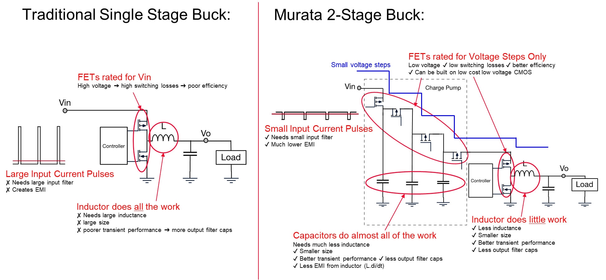
Figure 2 offers a closer look at the traditional single-stage buck compared to the two-stage buck architecture.
 Figure 2. A traditional single-stage buck converter compared to a Murata two-stage buck converter. (Image source: Murata).
Consider the more traditional single-stage buck approach in Figure 2 for a 12 Vin to 1 Vout scenario. The Vx node (mid-point of the FETs) is swinging from ground to Vin plus energy spikes stored in the leakage inductance and parasitics. This approach means that higher-voltage FETs are required, and EMI is likely to be an issue due to the rapid voltage change and ringing. The inductor is doing all the work and is a relatively high value, which negatively impacts the efficiency and transient response. Furthermore, the high-side FET is only conducting for 1/12th of the time in the 12:1 V scenario. This leads to a very high pulsing current on the input that requires additional decoupling to reduce the effects on conducted EMI. This very low duty cycle operation also limits the ability to run at very high switching frequencies.
Contrast this approach with the Murata two-stage implementation in Figure 2. The charge pump “staircases” the voltage down in integer steps—in this example, from 12 V to 8 V to 4 V—such that each stage sees only 4 V and can utilize low voltage, high-efficiency FET technology. The buck regulator is performing the last step in the conversion from 4:1 V. Most of the work has already been done by the first-stage capacitive charge pump. This architecture allows the second stage inductor to be reduced, which in turn enables a compact, low-profile design that can run at high frequencies with excellent transient response.
The first stage charge pump is implemented as two phases running out of phase at a 50% duty cycle. The second stage buck is running closer to a 25% duty cycle, which reduces input current and pulsating current. Both factors combine to minimize the input ripple and EMI profile of the converter. In summary, the two-stage architecture by Murata presents an improvement in efficiency, size and profile, and EMI.
For further information, please watch Murata’s webinar, “How Murata is changing the power density paradigm.”

Have questions or comments? Continue the conversation on TechForum, DigiKey's online community and technical resource.
Visit TechForum


