Why the Inter-Integrated Circuit (I2C) Bus Makes Connecting ICs So Easy—And How to Use It
Contributed By DigiKey's North American Editors
2020-04-07
Communications and control between integrated circuits using a parallel bus on a printed circuit board (pc board) is not practical. Even an 8-bit processor would require 16 lines just for data and many more for an address bus. It is even more problematic if multiple ICs need to be on a shared communications bus. There is not enough space for all those pc board trace runs. The solution is to link ICs using a serial communications bus such as the Inter-Integrated Circuit (I2C) bus, a two-wire serial bus that solves this problem.
This article will describe the origins of the I2C bus and how it operates to provide an efficient serial link between ICs. It will then discuss how the I2C bus is physically implemented, the protocol structure, and common applications of this ubiquitous communications bus. Example I2C interfaces and solutions from Microchip Technology will be used for demonstration purposes. The article will also discuss I2C similarities and differences with the System Management Bus (SMBus).
What is the I2C bus?
The I2C bus was developed by Phillips Semiconductors, now NXP Semiconductors, in the early 1980s as a simple bidirectional, two-wire bus for efficient communications and control of integrated circuits on a common pc board. The first specification was completed in 1992 and the bus has since become a de facto standard offered in components from over 50 IC manufacturers. This large deployment allows a systems approach to design where ICs can readily be included into the I2C bus structure without requiring custom design. Several other specialized buses such as the SMBus and the Power Management Bus (PMBus) along with several others share the basic architecture.
The I2C bus can link multiple ICs and sensors because it is an addressable bus; a seven- or ten-bit address field allows messages to be sent to a selected device by the master device. The original I2C had a maximum clock speed of 100 kilohertz (kHz), but over the years higher speed operating modes have pushed that limit to 3.4 megahertz (MHz).
The I2C bus uses two wires designated serial data line, or SDA, and serial clock line, or SCL. SDA and SCL are open drain/collector bidirectional lines and are connected to the positive power bus via a current source or a pullup resistor. Multiple devices can be connected to the bus, with the maximum number being limited by the bus capacitance. A master device controls the bus, and each device on the bus has a unique address. The master device can both transmit and receive data over the bus (Figure 1). I2C supports multi-master operation featuring collision detection and arbitration to prevent two or more master devices from initiating data transfers at the same time. However, this article will focus on single master configurations.
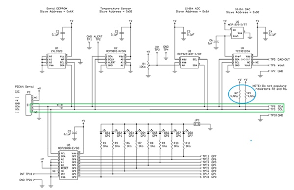 Figure 1: Schematic of a demonstration pc board from Microchip Technology which implements the I2C bus and connects it to five different devices. The master device is off board through connector P1. The SCL and SDA lines are outlined in green and the two pullup resistors are circled in blue. (Image source: Microchip Technology)
Figure 1 shows the schematic of a Microchip Technology PKSERIAL-I2C1 I2C demonstration board. This board implements the I2C bus using five different devices including an EEPROM, a temperature sensor, a 12-bit analog-to-digital converter (ADC), a 10-bit digital-to-analog converter (DAC), and an 8-bit serial-to-parallel converter. The master device is not on the board and is connected via connector P1. The SDA and SCL bus lines are outlined in green and the pullup resistors are circled in blue.
The SDA and SCL levels are, generally, a fixed percentage of the positive supply voltage, usually denoted as VDD. The reference levels are set at 70% and 30% of VDD for the logic “1” (high) and logic “0” (low), respectively.
Clock signals occur in bursts with one clock for each data bit transferred. Data on the SDA line must be valid while the clock is high. Data can be changed only while the clock is low.
From a designer’s point of view, new projects are simplified because the I2C interfaces are integrated into the ICs and there is no need to design an interface. Each device simply connects directly to the bus. ICs can be added or removed from the bus without affecting the other circuits (assuming the number of ICs in total doesn’t push the capacitance limit). The simple two-wire bus minimizes the number of pins on each IC and the number of runs on the pc board.
The I2C protocol
The bus is 8-bit oriented, communicating in bytes. As mentioned, the original maximum clock rate was 100 kHz in what is now referred to as Standard Mode. The bus now supports 400 kilobits per second (kbits/s) in Fast Mode, up to 1 Mega bit per second (Mbit/s) in Fast Mode Plus, and up to 3.4 Mbits/s in High Speed Mode (Hs-Mode).
The I2C protocol is best illustrated by looking at a typical transfer on the bus (Figure 2). The source of the screen image is a Teledyne LeCroy oscilloscope with low speed serial data trigger and decode option WS4KHD-EMB TD. This oscilloscope option can trigger and decode up to 19 low speed serial data interfaces including I2C.
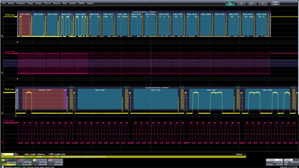 Figure 2: A typical I2C data packet consisting of a start bit, address field, acknowledge bit, 17 data bytes each with its own ACK bit, and finally a stop bit. Each field is identified by a color-coded overlay. The upper (yellow) trace is the whole SDA packet, beneath it is the SCL clock (red). The third and fourth traces are horizontally expanded views of both signals. (Image source: DigiKey)
The oscilloscope can trigger on specific serial events including start, stop, missing acknowledge (ACK), address, data, address plus data, frame length, and EEPROM data transfer. The protocol elements of the serial data standard are identified by a color-coded overlay. Each protocol field is decoded in either binary, hex, or ASCII with the selected code displayed within the overlay.
The SDA signal appears as a yellow trace while the SCL signal is shown as a red trace. The grey overlay box indicates the start and stop functions. The brick red overlay marks address data, the blue field is the packet data, and olive overlay boxes mark the ACK functions.
The top trace shows the entire I2C SDA packet from start to stop. Directly beneath it is the corresponding SCL signal. The third trace down is a time expanded zoom trace of the SDA signal, and beneath that is the synchronous SCL signal.
Both the SDA and SCL lines rest in the high state between transfers when the bus is free. The SCL signal consists of bursts of nine pulses at the clock rate, one for each data bit being transferred and one additional for the ACK bit.
All bus transactions start with a master generated start bit indicated in the zoomed SDA trace as a grey colored overlay box. Start is indicated by the master pulling the SDA line low while the SCL line is in a high state. Once the master issues the start bit the bus is considered busy. The master can issue multiple starts, a situation in which the subsequent starts are often called restarts.
All data transfers are 8 bits (one byte) in length, each followed by an ACK bit. Bits are transmitted with the most significant bit (MSB) first. Each byte transfer must be acknowledged. If the slave device is busy and cannot receive or transmit data, it can pull the SCL line low. This forces the master device into a wait state until the slave device releases the SCL line.
The ACK bit is formed after the transmitting device releases the SDA line before the ninth acknowledge clock pulse. If the receiving device has received the data byte, it pulls the SDA line low. In the zoom view of the SDA in Figure 2, there is a narrow spike just prior to the ninth clock pulse, which is the SDA line being released to return to the high state. The receiver pulls down the SDA line generating the ACK signal, which is marked symbolically by the olive box overlay. If the receiver does not pull the SDA line down before the ninth clock pulse, it is a not acknowledge (NACK) response. If a NACK occurs, the master can either generate a stop signal and abort the transfer or issue a repeated start to try again.
Immediately after the start condition, a slave address is issued. This is indicated by a brick red overlay box. There are two possible address formats; 7 bit or 10 bit, with the 7-bit address being the most common. The first 7 bits after the start represent the address data. The 8th bit indicates the data direction—either read or write. A write is indicated by the SDA line being in a low state, while having the SDA line high at this time indicates a read operation. 10-bit addressing uses the first two bytes after the start condition. I2C reserves several addresses for internal functions. The decode address data appears in the address overly box in binary, hex, or ASCII format.
The blue overlay fields mark the data transfers. Each one is eight bits long and is followed by an ACK/NACK response. The number of data bytes in an I2C packet is unlimited, but Figure 2 contains 17. The decoded data, like the address decode, appears in the data overlay box. The data stream is followed by a master generated Stop bit at the end of the data transfer, indicated by a grey overlay box in the top data trace. The stop bit is a low-to-high transition on the SDA line while the SCL line is in the high state. After the stop signal, the bus is again free.
The table at the bottom of the display summarizes all the information about the related data packet, including time since trigger, address length, address, read or write operation, packet length, and a summary of the data content. The number of entries in the table matches the number of I2C packets acquired by the scope, which in this case is only a single line.
If a protocol error occurs, it is indicated by a bright red box behind the other protocol overlay boxes.
I2C devices
One of the biggest advantages of the I2C bus is the extremely large number of devices that have incorporated it into their design. The Microchip Technologies demo board provides some examples of the types of ICs that incorporate the I2C bus or one of its derivatives like the SMBus.
Microchip Technology’s PIC16F677 is an 8-bit microcontroller that finds use in many embedded designs. It implements a Synchronous Serial Port that can be controlled to communicate with either the serial peripheral interface (SPI) or I2C to other controllers or peripheral devices (Figure 3).
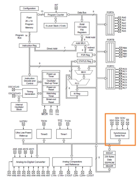 Figure 3: The Microchip Technology PIC16F677 is an 8-bit microcontroller that includes a Synchronous Serial Port (outlined in orange) capable of being programmed as either an SPI or an I2C bus. (Image source: Microchip Technology)
This microcontroller supports both master and slave mode of I2C using 7- or 10-bit addressing. It uses the SCK/SCL pin for the I2C SCL clock signal and the SDI/SDA pin for the data signal.
These two pins are connected to the SCL and SDA lines on the I2C bus to enable communication with other devices. A common connection is to an I2C-based sensor such as Microchip Technology’s TCN75AVOA713 two-wire serial temperature sensor (Figure 4).
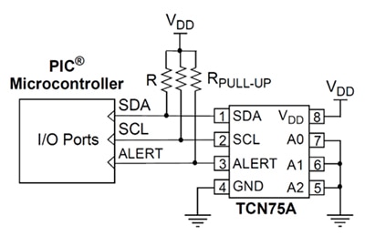 Figure 4: The Microchip Technology TCN75A temperature sensor is directly connected to the PIC16F677 microcontroller to communicate temperature data. (Image source: Microchip Technology)
Having serial communications capability, this temperature sensor has increased functionality. Its internal user-programable registers can be used to set the temperature measurement resolution, power saving shutdown mode, and even set the alert output to indicate when the temperature range exceeds preset limits.
There are also a number of devices that decode the I2C serial data stream and break it out into parallel data. Consider the Microchip Technology MIC74YQS-TR 2-wire I/O expander and fan controller (Figure 5).
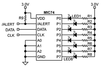 Figure 5: The Microchip Technology MIC74YQS-TR I/O expander converts the serial data stream into eight independent parallel I/O lines. (Image source: Microchip Technology)
This IC is a fully programmable I/O expander providing eight independent I/O Lines. The I/O lines can be individually programmed as an input or an output. Figure 5 shows the MIC74YQS-TR driving eight LEDs under the control of the serial bus. This is similar to the use of the MCO23008 on the I2C demo board in Figure 1. The MIC74YQS-TR, in conjunction with a power regulator, can also implement a fan motor speed control using its four most significant bits.
SMBus and I2C
The serial input to the I/O expander is designed for the SMBus, but it is also compatible with the I2C bus. The SMBus specification is based on I2C and was defined by Intel and Duracell in 1994. The primary difference is that standard mode I2C logic levels are relative to VDD and those of SMBus are fixed. In most cases, with VDD between 3 volts and 5 volts, experience has shown that this is not an issue.
Another difference is that SMBus is limited to clock rates of 100 kHz or less, while I2C has several modes that support higher clock rates. When dealing with bus compatibility, this limits the maximum clock rate to 100 kHz or the I2C standard clock mode.
So, except for very special situations, SMBus and I2C are compatible.
Conclusion
The I2C bus and its derivatives are pervasive in hundreds of ICs of all types making it easy to connect them in multifaceted designs and applications. Coupling mixed signal and analog sensors expands the scope of microcontroller-based embedded systems. All this through a simple, two-wire serial digital interface.

Disclaimer: The opinions, beliefs, and viewpoints expressed by the various authors and/or forum participants on this website do not necessarily reflect the opinions, beliefs, and viewpoints of DigiKey or official policies of DigiKey.


