Use a Dual-Path ADC Architecture for Low-Noise Wideband Signal Capture
Contributed By DigiKey's North American Editors
2026-02-19
Time-domain instrumentation applications such as time-of-flight mass spectrometry (TOF-MS), distributed fiber-optic sensing, optical coherence tomography, and high-speed oscilloscopes require accurate signal capture from direct current (DC) to multi-gigahertz (GHz) frequencies. Conventional high-speed digitizer architectures face a fundamental limitation on measurement accuracy due to the noise inherent in analog-to-digital converters (ADCs), forcing designers to compromise between precision and wideband capture.
This article provides a brief introduction to the digitization challenges designers of time-domain instrumentation face. It then introduces a high-performance digitizer from Analog Devices and shows how designers can use this board and its development resources for a successful implementation.
How wideband digitization challenges affect time-domain instrumentation
Time-domain instrumentation applications share a common requirement for precision digitization across a wide bandwidth. In TOF-MS, for example (Figure 1), digitization provides the foundation for sample identification. Here, ions from a sample are accelerated through the vacuum maintained in the flight tube, where they achieve different velocities depending on their mass-to-charge ratio. Each cluster of ions with the same mass-to-charge ratio arrives at the detector as a pulse as narrow as a few hundred picoseconds (ps).
 Figure 1: In TOF-MS, ions accelerated to the same kinetic energy travel at different velocities based on mass, with lighter ions arriving at the detector first, enabling calculation of mass directly from flight time. (Image source: Analog Devices)
TOF-MS relies on its high-performance ADC subsystem to reliably digitize the pulse and determine its peak, which represents the arrival time of each ion cluster and thus the mass of that type of ion. Because each sample is critical in determining this peak, the ADC subsystem needs to deliver gigasamples per second (Gsamples/s) rates to capture sufficient samples.
High-speed oscilloscopes and distributed fiber-optic sensing face similar demands for accurate, high-bandwidth signal measurement. High-speed oscilloscopes require the accurate capture of fast transients while maintaining DC baseline fidelity. Distributed fiber-optic sensing systems share the need for wideband capture with low noise across the full measurement bandwidth, from near-DC to several gigahertz.
The challenge in these and other applications is ensuring both wide bandwidth and precision measurement, even at lower frequencies where 1/f noise degrades the performance of radio-frequency (RF) ADCs. Optimized for RF signal capture, this class of ADCs delivers the bandwidth required but exhibits elevated 1/f noise at low frequencies below its 1/f corner (Figure 2).
 Figure 2: The 1/f noise inherent in ADCs increases at frequencies below the 1/f corner, limiting measurement accuracy. (Image source: Analog Devices)
Noise increases as frequency decreases, resulting in a degraded signal-to-noise ratio (SNR) and increased measurement uncertainty at low frequencies, even when the ADC performs well at gigahertz frequencies. Precision ADCs minimize 1/f noise through architectural features such as chopper stabilization, auto-zeroing, and correlated double sampling, which prioritize low-frequency accuracy over wideband performance, precluding their use at GHz bandwidths.
Addressing this fundamental tradeoff requires the novel dual-path ADC architecture used in Analog Devices' ADMX6001-EBZ evaluation board.
How the ADMX6001 dual-path architecture achieves wideband precision
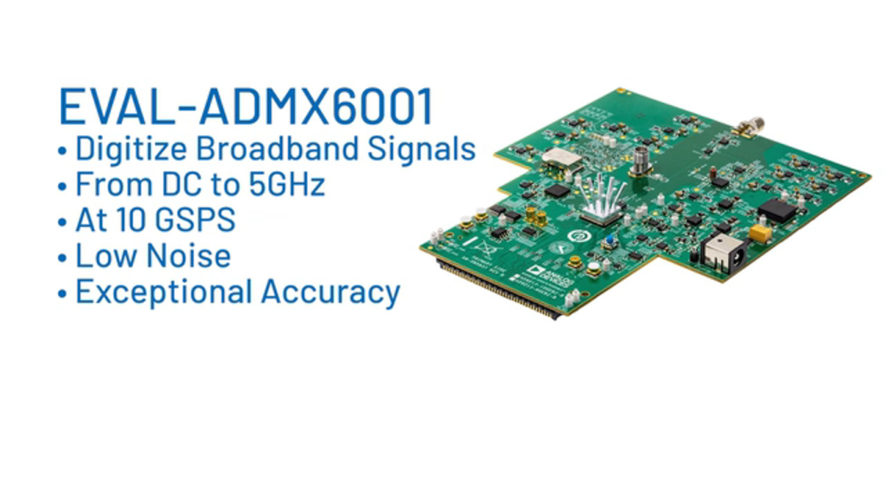
The ADMX6001-EBZ evaluation board is a DC-coupled, 10 Gsamples/s digitizer and complete reference design for custom low-noise, high-bandwidth precision digitizers. It resolves the bandwidth-versus-precision tradeoff through a dual-path architecture comprising a high-speed ADC path optimized for wideband capture and a precision ADC path optimized for low-frequency accuracy. By combining data from these two paths, the board compensates for 1/f noise in high-speed ADCs, maintaining accurate signal digitization from DC to 5 GHz.
The high-speed path centers on Analog Devices' AD9213 12-bit RF ADC (Figure 3), which can sample at 10 Gsamples/s. Designed to deliver wide instantaneous bandwidth and low conversion error rates, the AD9213 is based on a multistage, differential, pipelined ADC core with output error correction. To ensure maximum bandwidth and deterministic output latency, its output stage integrates a 16-lane JESD204B interface. Besides providing line rates of 16 gigabits per second (Gbits/s), the output stage employs standard JESD204B mechanisms to maintain deterministic latency between the AD9213's output and a host controller's JESD204B input.
 Figure 3: The AD9213 integrates a multistage, differential, pipelined ADC core with output error correction and a 16-lane JESD204B interface supporting line rates up to 16 Gbits/s. (Image source: Analog Devices)
This ADC delivers the high dynamic performance required for accurate high-frequency signal capture. At 10 Gsamples/s with a 1000 MHz input at -1 decibels relative to full scale (dBFS), the AD9213 exhibits an SNR of 55.8 dBFS and a spurious free dynamic range (SFDR) of 70 dBFS (typical). Furthermore, this device maintains excellent SNR and SFDR across input frequencies from 100 MHz to beyond 6 GHz (Figure 4), meeting the demand for wideband accuracy.
 Figure 4: The AD9213 maintains high SNR and SFDR performance across input frequencies from 100 MHz to beyond 6 GHz, providing the wideband capture capability required for time-domain instrumentation. (Image source: Analog Devices)
The precision path uses Analog Devices' AD4080, a 20-bit, 40 megasamples per second (Msamples/s) differential successive approximation register (SAR) ADC with integrated event detection, a digital filter, and a dual-input sampler to ensure precision conversion at high sampling rates. Its output stage provides direct access to conversion results and to a 16,384-sample first-in-first-out (FIFO) through an interface supporting both Serial Peripheral Interface (SPI) and low-voltage differential signaling (LVDS) output. As with the AD9213, the AD4080 provides integrated capabilities designed to help ensure alignment with the host controller and account for system propagation delays. Where the AD9213 provides the required bandwidth, the AD4080 delivers the required low-frequency precision. At 1 kilohertz (kHz), the AD4080 achieves 93.6 dB SNR and -110.2 dB total harmonic distortion (THD) (Figure 5).
 Figure 5: At 1 kHz, the AD4080 achieves 93.6 dB SNR and -110.2 dB THD, demonstrating the low-frequency precision that complements the AD9213's wideband capture. (Image source: Analog Devices)
The ADMX6001-EBZ board addresses the need in time-domain instruments to handle single-ended, unipolar, or bipolar input signals at different DC levels. Along with a high-speed ADC driver for single-ended-to-differential conversion, a precision digital-to-analog converter (DAC) biases the ADC driver to provide an adjustable DC offset, maximizing the high-speed AD9213's dynamic range. This capability is essential in applications such as TOF-MS, where proper DC offset adjustment ensures the ADC's full dynamic range is available for pulsed ion signals.
Accelerating evaluation and development with a companion board and software
Analog Devices designed the ADMX6001-EBZ evaluation board to work with AMD/Xilinx's VCU118 (EK-U1-VCU118-G) evaluation kit (Figure 6). Based on a high-performance field-programmable gate array (FPGA), the kit provides the resources and processing capability needed to acquire and combine the dual-path data streams. For normal digitizing operations, the ADMX6001-EBZ board connects to the VCU118 through an enhanced high-throughput FPGA mezzanine card (FMC+) high serial pin connector (HSPC), using a small benchtop fan for sustained operation.
 Figure 6: The ADMX6001-EBZ evaluation board connects to the VCU118 kit through a high-throughput FMC+ HSPC connector, providing a complete hardware platform for evaluating dual-path digitization performance. (Image source: Analog Devices)
Intellectual property (IP) cores and memory blocks instantiated in the VCU118's FPGA matrix implement the separate high-speed JESD204B and LVDS interfaces needed to receive the dual data streams from the high-speed AD9213 and precision AD4080. Both data streams are fed into FPGA memory buffers before being transferred to system memory for subsequent merging and application-specific processing.
For evaluating the ADMX6001-EBZ board and signal digitization, Analog Devices provides its IIO Oscilloscope graphical user interface (GUI) tool and its comprehensive PyADI-IIO Python library. The IIO Oscilloscope tool is a cross-platform GUI for interactively modifying board settings, capturing data, and plotting the results. For example, to enable the AD9213's DC-coupled mode, designers would use an IIO Oscilloscope tool panel (Figure 7) to specify the device (AD9213 in this case), register of interest (0x1617 here), and its value (0x1).
 Figure 7: The IIO Oscilloscope GUI provides direct register access for configuring ADC operating modes, shown here enabling the AD9213's DC-coupled mode by writing 0x1 to register 0x1617. (Image source: Analog Devices)
The PyADI-IIO library provides an application programming interface (API) to board functionality, built around a Python class (Hammerhead) that initializes the board to default settings and provides methods that abstract low-level operations for setting the offset, capturing data from each ADC, and plotting the results.
Sample code, such as the PyADI-IIO library's ADMX6001_acquisition.py script, demonstrates basic design patterns for using these methods for more complex evaluation sequences. For example, to digitize an input signal at different DC offsets, designers import the Hammerhead class from the library's ADMX6001_MultiClass_pCal module and create an instance of it. Designers need only a few lines of code, using that instance’s methods, to evaluate the ADMX6001-EBZ board's ability to capture samples at different DC offsets (Listing 1).
Copy
import adi
import matplotlib.pyplot as plt
import numpy as np
import time as dt
import ADMX6001_MultiClass_pCal as HMC
from scipy.fft import fft, rfftfreq

# Initialize ADMX6001 board
HH = HMC.Hammerhead("ip:192.168.2.1")
…
dac_offset1 = 0
HH.set_dac_offset(dac_offset1)
hispeed_data1 = HH.capture_data_ad9213(2**16) # Capture specified # of samples @ 10GSPS
HH.plot_data_ad9213(hispeed_data1) # Plot data captured by high speed path
…
dac_offset2 = 200  # Set offset voltage in mV
HH.set_dac_offset(dac_offset2) # Set offset voltage in mV
hispeed_data2 = HH.capture_data_ad9213(2**16) # Capture specified # of samples @ 10GSPS
HH.plot_data_ad9213(hispeed_data2) # Plot data captured by high speed path
…
dac_offset3 = -200  # Set offset voltage in mV
HH.set_dac_offset(dac_offset3) # Set offset voltage in mV
hispeed_data3 = HH.capture_data_ad9213(2**16) # Capture specified # of samples @ 10GSPS
HH.plot_data_ad9213(hispeed_data3) # Plot data captured by high speed path

# plot three AD9213 acquisitions with different dc bias/offset
x_time = np.arange(0, len(hispeed_data1))*(10**(-4))
fig, (ax) = plt.subplots(1, 1)
ax.plot(x_time, hispeed_data1, label=str(dac_offset1) + 'mV offset')
ax.plot(x_time, hispeed_data2, label=str(dac_offset2) + 'mV offset')
ax.plot(x_time, hispeed_data3, label=str(dac_offset3) + 'mV offset')
Listing 1: As illustrated by this code snippet from the PyADI-IIO library, designers need only a few lines of code to evaluate the ADMX6001-EBZ board's ability to capture samples at different DC offsets. (Code source: Analog Devices)
Plotting the data captured from the same input signal at three DC offset settings (0 millivolts (mV), 200 mV, -200 mV) demonstrates the ADMX6001-EBZ board's ability to adjust the input bias to optimize the high-speed ADC's dynamic range utilization (Figure 8).
 Figure 8: Plotting the data captured from the same input signal at three DC offset settings (0 mV, 200 mV, -200 mV) demonstrates the ADMX6001-EBZ board's ability to adjust the input bias to optimize the high-speed ADC's dynamic range utilization. (Image source: Analog Devices)
Together, these two tools accelerate evaluation and development. While the IIO Oscilloscope GUI provides a quick, interactive way to verify different register settings and capture options, the PyADI-IIO library enables the implementation of more complex sequences of operations.
Conclusion
Instrumentation applications that require accurate digitization from DC through multi-gigahertz frequencies force designers to compromise between wideband capture and low-frequency precision. The ADMX6001-EBZ DC-coupled 10 GSPS digitizer evaluation board from Analog Devices resolves this tradeoff through a dual-path architecture. Paired with an FPGA development kit and software tools, this board provides an evaluation platform and a complete reference design that accelerates the development of precision wideband digitizers for demanding time-domain applications.
References:
Disclaimer: The opinions, beliefs, and viewpoints expressed by the various authors and/or forum participants on this website do not necessarily reflect the opinions, beliefs, and viewpoints of DigiKey or official policies of DigiKey.