The Basics of Anti-Aliasing Low-Pass Filters (and Why They Need to be Matched to the ADC)
Contributed By DigiKey's North American Editors
2020-03-24
Basic sampled data acquisition systems—whether they are for IoT, smart homes, or industrial control—if not protected will suffer from inaccuracies due to aliasing, where spurious signals are generated due to under sampling the analog input. Aliasing folds signal components at frequencies above the Nyquist frequency (half the sampling frequency) back into the baseband spectrum where they cannot be separated from the desired signals, leading to errors. Additionally, noise above the Nyquist frequency is also mixed down into the baseband, lowering the signal to noise ratio (SNR) of the desired baseband signals.
The solution to prevent aliasing is to band limit the input signals—limiting all input signal components below one half of the analog to digital converter’s (ADC’s) sampling frequency. Band limiting is accomplished by using analog low-pass filters that are called anti-aliasing filters. These filters must band limit without adding signal distortion, noise, or amplitude variations with frequency. Anti-aliasing low-pass filter designs must provide fast roll off with sufficient stop band attenuation to lower signal amplitudes sharply above the Nyquist frequency.
This article discusses the design criteria for anti-aliasing low-pass filters and why and how they are carefully matched to the specifications of the ADC. It will then show how they can be implemented with active or switched capacitor filter elements using sample devices from Analog Devices.
What is aliasing?
Aliasing occurs when a system acquires data at an insufficient sampling rate. If a signal contains any frequencies greater than the Nyquist frequency, they are mixed with the sampling frequency in the converter's sampler and mapped to frequencies less than the Nyquist frequency, causing different signals to become mixed and indistinguishable from each other (i.e., aliases of one another) during sampling (Figure 1).
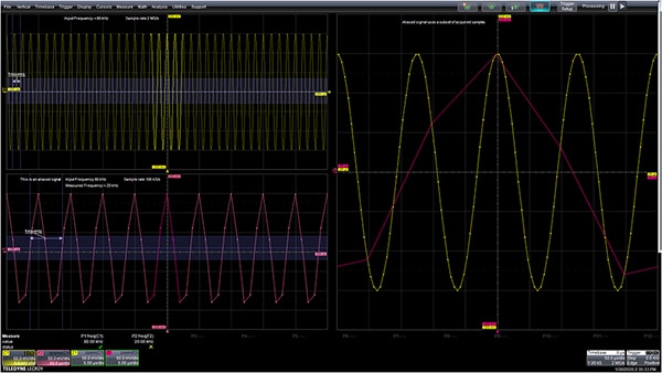 Figure 1: An example of aliasing. An 80 kilohertz (kHz) sine wave sampled at 2 mega samples per second (upper left) shows no aliasing. Reducing the sample rate to 100 kilosamples per second (lower left) results in the signal being interpreted as having a frequency of 20 kHz. Both the properly sampled and aliased signals are overlapped in the zoom view (right). Dots on that trace show the sample locations. Note that the aliased signal uses a subset of the correctly sampled data. (Image source: DigiKey)
The signal shown in the upper left grid is an 80 kHz sine sampled at 2 mega samples per second (MS/s). At 2 MS/s the Nyquist frequency is 1 megahertz (MHz); the signal is well below that. The lower left grid shows what happens when the sample rate is reduced to 100 kilosamples per second (kS/s). The Nyquist frequency is now 50 kHz and the frequency of the 80 kHz sine is now above the Nyquist frequency and is aliased.
On the right side of the image, the properly sampled and aliased signals are horizontally expanded and overlapped, and real samples are indicated by a dot. Note that the aliased signal contains a subset of the samples of the signal sampled at 2 MS/s. Sampling is a mixing operation and the output of the operation consists of the sum and difference of the input signals and sampling frequency.
At a sample rate of 100 kS/s and an 80 kHz signal frequency, the difference frequency is 20 kHz. Frequency measurements of both cases are shown beneath the display grids. The parameter readout P1 reads the properly sampled signal frequency of 80 kHz, while the frequency of the aliased signal is 20 kHz.
Designing an anti-aliasing low-pass filter
The first step when designing an anti-aliasing filter is to determine the bandwidth required in the acquisition system. This sets the cutoff frequency of the low-pass filter. Filter cutoff frequencies are typically set to the -3 decibel (dB), or half power point. This is the frequency where the filtered signal amplitude falls to 0.707 of the amplitude at DC. If the acquisition system design requires a flatter frequency response, the cutoff might be defined with a lower attenuation value—for instance, -1 dB. A higher cutoff frequency amplitude places more importance on the roll off of the anti-aliasing filter’s frequency response.
Having determined the bandwidth of the acquisition system, the sampling rate can be set. The theoretical minimum sampling frequency is twice the acquisition system bandwidth. This theoretical limit is not a good sampling frequency in practice, however, since a realizable anti-aliasing filter cannot attenuate signals above the cutoff frequency as abruptly as that of a perfect theoretical filter. This means that the sample rate should be higher. The trade-off here is that memory requirements increase along with higher sampling frequency. In the days of expensive memory this kept the sampling rate as close to Nyquist as possible—usually between 2.5 and four times the input bandwidth. Lower cost memory eases this requirement, so the sample rate can be higher; five or ten times the bandwidth is not unheard of.
Consider a design for an ultrasonic sensor requiring an acquisition bandwidth of 100 kHz. The sampling rate could be 500 kHz to 1 MHz.
Now the ADC can be chosen. For our example a 12-bit successive approximation converter with a sample rate of 1 MS/s, like the Analog Devices LTC2365ITS8#TRMPB, can be chosen. Its 12-bit resolution provides a theoretical dynamic range of 72 dB. This ADC has outstanding dynamic performance that includes a signal to noise and distortion (SINAD) specification of -72 dB and a SNR of -73 dB, both at a sampling frequency of 1 MS/s (Figure 2).
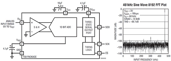 Figure 2: The block diagram and SINAD performance of the Analog Devices LTC2365ITS8#TRMPB 12-bit successive approximation ADC. (Image source: Analog Devices)
Operating at a sampling rate of 1 MS/s, the Nyquist frequency is 500 kHz. The output of the 100 kHz low-pass filter has to have a stop band attenuation to bring signal components above Nyquist down to the ADC noise floor—in this case greater than -73 dB for frequencies greater than 500 kHz.
Selecting a filter type
There are many possible low-pass filter types or configurations. The most commonly used are Butterworth, Chebyshev, and Bessel filters. The frequency responses of these filters differ, and they offer some key differentiators depending on the application (Figure 3).
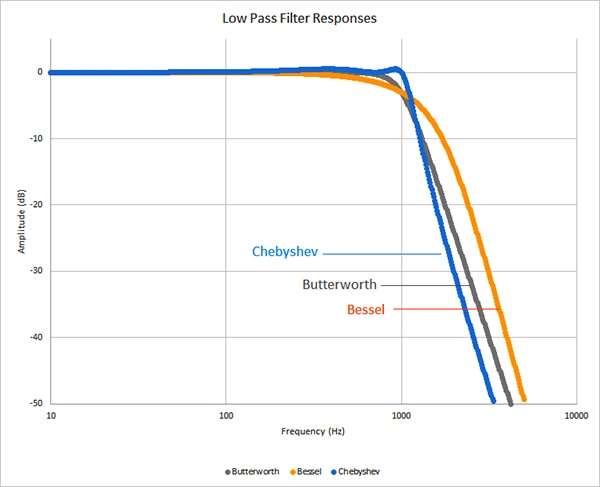 Figure 3: A comparison of Butterworth (gray), Chebyshev (blue), and Bessel (orange) filter frequency responses. The filter types differ in passband flatness, phase delay, and slope of the transition region. (Image source: DigiKey)
The three filter responses shown have specific characteristics. For example, the Butterworth filter has a maximally flat amplitude response. This means it offers the flattest gain response with frequency in the passband with moderate roll-off in the transition region.
Bessel filters offer uniform time delay for constant group delay. This means they have linear phase response with frequency and excellent transient response for a pulse input. This excellent phase response comes at the expense of flatness in the passband and a slower initial roll off attenuation beyond the passband.
Chebyshev filters are designed to present a steeper roll-off in the transition region but have more ripple in the passband. Designs using this filter type are generally based on a specific maximum ripple. For instance, if the cutoff frequency amplitude limit is -1 dB, then the ripple specification usually would be set to 1 dB maximum.
The response of these filters to a pulse in the time domain is useful in understanding the appropriate filter type selection (Figure 4).
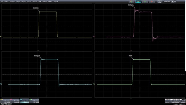 Figure 4: Filter response to an input pulse (upper left) shows the differences in time domain pulse response of the Chebyshev (upper right), Butterworth (lower left), and Bessel (lower right) filter types. (Image source: DigiKey)
The Bessel filter’s linear phase response with frequency passes the pulse with minimal distortion, but it doesn’t have the amplitude flatness of the Butterworth filter or the sharp cutoff of the Chebyshev filters. The type of filter selected depends on the application:
- The Butterworth filter should be chosen if amplitude accuracy is the paramount concern
- The Chebyshev filter would be the filter of choice if the desired sampling rate is close to the signal bandwidth
- The Bessel filter is the best choice if pulse fidelity is the primary concern
Filter order
Filter order refers to the complexity of the filter design. The term relates to the number of reactive elements, such as capacitors, in the design. It also represents the number of poles in the filter’s transfer function.
The order of a filter affects the steepness of the transition region roll-off and hence the width of the transition region. A first-order filter has a roll-off of 6 dB per octave, or 20 dB per decade. A filter of the nth order will have a roll-off rate of 6×n dB/octave or 20×n dB/decade. So, an 8th-order filter has a roll-off rate of 48 dB per octave or 160 dB per decade.
Using the ultrasonic sensor design described earlier as an example, all signals higher than 100 kHz need to be attenuated by at least -73 dB by the Nyquist frequency of 500 kHz. The 8th-order filter attenuates signals by about -98 dB at 500 kHz (Figure 5). A 6th-order filter attenuates an out-of-band signal at 500 kHz by about -83 dB. So, for our example a 6th-order filter would be adequate, but an 8th-order filter would provide an even lower amplitude for out-of-band signals. If the costs are the same, the 8th-order filter should be chosen. More on this trade-off later when components are discussed.
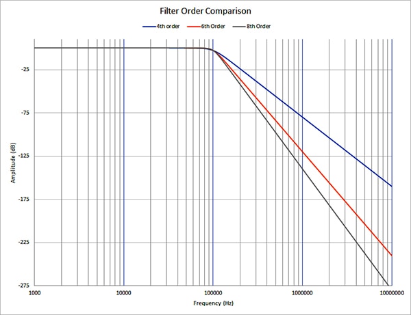 Figure 5: Comparing the roll-off of 4th (blue), 6th (orange), and 8th-order (gray) filter responses. (Image source: DigiKey)
The order of a filter can be increased by cascading multiple filter sections. For example, two 2nd-order low-pass filters can be cascaded together to produce a fourth-order low-pass filter, and so on. The trade-off in cascading multiple active filters is an increase in power consumption, cost, and size.
The choice of a 6th or 8th-order filter will also depend on the configurability of the filter component selected. Filter ICs configured as quad 2nd-order filters can implement a 6th-order filter, but filter ICs configured as dual 4th-order filters would have to implement an 8th-order filter.
Filter components
Anti-aliasing filters for acoustic and ultrasound frequencies can be implemented using active or switched capacitor filters. Generally, the results of using either filter type are very similar. In applications using very-high-resolution ADCs of 16 or more bit resolution, the active filter may be preferred due to a lower potential for noise. Switched capacitor filters, which require a clock signal, have a higher potential for noise due to cross talk from the clock signal.
The Analog Devices LTC1563 family offers 4-pole or 4th-order active filters that use a single resistor to control the cutoff frequency. The family offers both Butterworth and Bessel type filter configurations. The LTC1563-2 is a 4-pole Butterworth configured filter component with a maximum cutoff frequency of 256 kHz. This filter IC can be cascaded to obtain an 8th-order low-pass response (Figure 6).
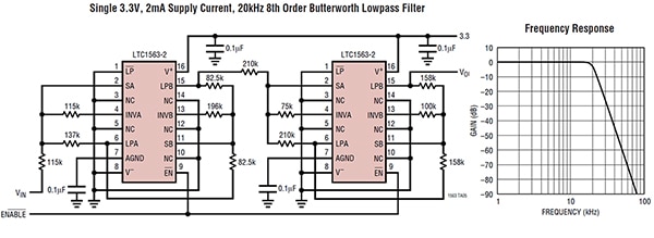 Figure 6: An 8th-order, 20 kHz Butterworth filter implemented using two Analog devices LTC1563-2 devices. (Image Source: Analog Devices)
If the application requires a variable cutoff frequency, the Analog Devices LTC1564IG#TRPBF is a good choice. This 8th-order low-pass filter has a bandwidth that is digitally controlled using a 4-bit control bus to vary the cutoff frequency from 10 kHz to 150 kHz in 10 kHz steps. The gain is also digitally programmable. The filter has 122 dB of dynamic range and is intended for acquisition systems of 16 to 20-bit resolution (Figure 7).
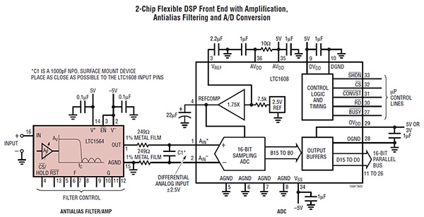 Figure 7: A 16-bit, 500 kS/s acquisition system using only two ICs. The LTC1564IG#TRPBF provides variable bandwidth to 150 kHz and gain up to 24 dB. (Image source: Analog Devices)
Variable cutoff frequency designs can also be implemented with switched capacitor filters. The Analog Devices LTC1068-25IG#PBF is a universal switched capacitor 8th-order low-pass filter with a maximum cutoff frequency of 200 kHz. This IC consists of four 2nd-order filter building blocks that can be cascaded to create an 8th-order low-pass filter (Figure 8).
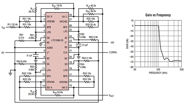 Figure 8: An 8th-order low-pass filter using an LTC1068-25IG#PBF switched capacitor filter. The cutoff frequency is set using the switching clock and is equal to the switching clock frequency divided by 32. (Image source: Analog Devices)
Universal active filter ICs can also be used for anti-aliasing. They require a greater number of components to set the filter characteristics. The Analog Devices LTC1562-2 is a low noise/low distortion quad 2nd-order filter that can be configured as a Butterworth, Chebyshev, elliptic, or equiripple delay response filter with low-pass, high-pass, or bandpass response. Cutoff frequencies are from 20 to 300 kHz using resistor value programming. Three resistors program the center frequency, gain, and Q. This filter design of quad 2nd-order filters can be configured to produce filters of 2nd, 4th, 6th, or 8th order.
Conclusion
Anti-aliasing low-pass filters are required for data acquisitions systems to ensure that all sampled signals of interest can be reconstructed accurately. The filter characteristics required are determined by the bandwidth, amplitude resolution, and sampling rate of the ADC with which it is paired. As shown, there are multiple design options for implementing the low-pass filter including active, digitally controllable, and switched capacitor devices.

Disclaimer: The opinions, beliefs, and viewpoints expressed by the various authors and/or forum participants on this website do not necessarily reflect the opinions, beliefs, and viewpoints of DigiKey or official policies of DigiKey.


