Powering DDR Memory
Contributed By Electronic Products
2013-12-17
Inexpensive-to-manufacture double data rate (DDR) memory (and later variants such as DDR2 and DDR3) has provided the mainstay for working memory in desktop and laptop computers. By clocking the memory on both the leading and trailing edge of the pulse train, memory throughput is doubled with only a marginal increase in power dissipation.
However, to make the most of this throughput and avoid common problems with such a high-frequency scheme, for example, ringing and reflections that can inadvertently trigger logic devices, bus termination circuitry requires its own power supply. To operate efficiently, this power supply must provide exactly half of the input voltage of the main memory chipset supply while being able to both source and sink current.
This article describes the unique demands on the power supplies for DDR memory and then examines some dedicated power controllers from major suppliers that ease the design engineer’s challenge.
Special requirements for DDR
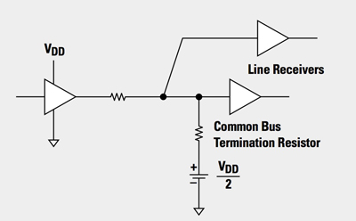
Figure 1 illustrates a popular termination scheme for a computer clock distribution network designed to prevent spurious ringing and reflection that could inadvertently trigger logic devices attached to the bus. An additional advantage of this topology is that it halves the power dissipated in the clock network (when the bus is high half the time and low at other times) compared to simply terminating the line via a resistor straight to ground. The trade-off is the requirement for an additional power supply to generate VDD/2.

The termination resistor is connected to a second supply voltage (VTT) that is equal to half of the main supply voltage (VDD). The result of connecting a second voltage is that power dissipation in the termination resistor is then constant regardless of the supply voltage and is equal to VTT (or VDD/2) squared divided by the termination resistance (from P = V²/R).
However, the demands on the secondary power supply are unusual. Apart from the supply voltage (VTT) being one half of the main supply voltage (VDD), the device needs to both source and sink current (Figure 2). When VDD is low, current flows from the VTT supply into the driver. However, when VDD is high, current flows from the driver to the VTT supply. It is also important that the VTT supply switches smoothly between states to avoid inefficiencies that increase power dissipation.

A synchronous switching DC/DC voltage regulator is typically used for the VTT power supply because it is more efficient than a linear low drop-out regulator (LDO) (although some designers favor an LDO because it is easier to incorporate into the power supply design). However, maintaining high efficiency (low power dissipation) and good transient response in these two different operating modes is a challenge.
In a synchronous switching buck regulator, the transition from the point where the high-side MOSFET conducts to that where the low-side device conducts is carefully controlled. The high- to low-side transition can be made almost without loss. In practice, the high-side switch is first turned off, which allows the external energy-storing inductor to swing the phase voltage to zero. By using a comparator to sense the phase voltage and then turning the bottom switch on while it is exposed to no voltage, zero-voltage switching can be achieved for both devices. In contrast, the transition from low- to high-side is “hard switched” and some inefficiencies are incurred because the phase voltage must be switched while positive, resulting in some cross conduction and capacitive loss.¹
However, in boost mode the opposite is true: the zero-voltage switching occurs during the low- to high-side transition and the hard switching occurs when the inductor is pulled low. Power supply designers have come up with some clever tricks to overcome the hard-switching inefficiencies that work well when a power supply operates in a buck or boost configuration for long periods, and rarely, if ever, switches between the two modes.
The constant rapid flipping between buck and boost operation (sourcing and sinking current) of the secondary voltage regulator in a DDR memory circuit, while the device maintains a constant output voltage of half the main supply (VDD) independent of input voltage and output current, demands a different type of control regime compared with that used for conventional power supplies if high efficiency is to be preserved.
Control modules for DDR power supplies
Fortunately, the DDR power supply designer does not have to worry about coming up with a control regime as several key semiconductor vendors have already turned their attention to the task and have commercialized controllers that meet the unique demands of DDR memory power supply.
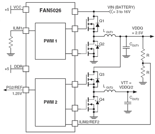
Fairchild Semiconductor offers their FAN5026 Dual DDR/Dual Output Switching Controller for memory applications. The device is designed to operate as a dual pulse width modulation (PWM) controller driving two synchronous switching regulators.
In DDR mode, one channel tracks the output voltage of another and provides the necessary output current sink and source capability. The device offers two outputs for the main power supply (VDD) and a secondary supply (VTT) that tracks VDD/2. The chip can operate from an input range of 3 to 16 V and the company says that the device provides high efficiency and regulation for the two output voltages adjustable in the range of 0.9 to 5.5 V. Synchronous rectification and hysteretic operation maintain efficiency at light loads.
The module is targeted at applications such as server- and desktop-DDR memory power or graphics card power requirements. Figure 3 shows an application circuit for the FAN5026.

Texas Instruments also offers a DDR and DDR2 controller module, the TPS51020. The chip can operate from a 4.5 to 28 V input and is specifically designed for high-performance, high-efficiency applications where the loss associated with a current-sense resistor is unacceptable. Examples include Li-ion battery-powered portable computers. High efficiency at light load conditions can be maintained by enabling an autoskip operation in the PWM train (Figure 4).

The company says the device provides a one-chip solution for a dual switching regulator DDR power supply. In DDR mode, the TPS51020 provides all the functionality required for the DDR application including VDD/2 tracking for VTT, current source and sink capability, and a VTT reference output.
For their part, Linear Technology offers the LTC3876 as a complete DDR power solution. The device is compatible with DDR, DDR2, DDR3, and future DDRX lower-voltage standards, integrates VDD and VTT controllers and a precision linear VTT reference. The company says a differential output sense amplifier and precision internal reference combine to offer an accurate VDD supply.
The VTT controller tracks the precision VTT reference with less than 20 mV total DC error. The reference maintains 1.2 percent regulation accuracy when tracking VDD/2. The LTC3876 has an input range of 4.5 to 38 V, and VDD can range from 1.0 to 2.5 V, with a corresponding VTT output range of 0.5 to 1.25 V.
DDR memory and its later variants have enabled modern computers to operate at high speed without dramatically increasing power dissipation. However, powering the chipset and terminating the common bus requires careful design if spurious signals are to be avoided at the high frequency at which DDR runs. Fortunately, engineers can obtain a significant head start on their power supply design by selecting one of the commercial DDR power supply modules on the market. These devices incorporate all the functionality required to power both the memory chipset and to supply a constant halved voltage for the termination trace that precisely tracks the main power supply.
For more information about the parts described in this article, use the links provided to access product pages on the DigiKey website.
References:
- “Power supply solution for DDR bus termination,” Robert Kollman, John Betten, and Bang S. Lee, Texas Instruments, Analog Applications Journal, July 2001.
Disclaimer: The opinions, beliefs, and viewpoints expressed by the various authors and/or forum participants on this website do not necessarily reflect the opinions, beliefs, and viewpoints of DigiKey or official policies of DigiKey.


