How to Combine High and Low Voltages in a Single Design
Contributed By DigiKey's North American Editors
2018-04-10
While there tends to be much emphasis on lower voltages to reduce power, designers often need to incorporate both low and high voltages in the same design. This presents three challenges: developing the higher voltage DC rail; providing higher voltage analog amplifier/driver functions; and meeting the relevant safety and regulatory mandates for higher voltage systems.
The advantages of low voltage, sub 5 volt operation are many, including lower power consumption, lower losses due to heat generation, higher IC functional density, extended run times and longer life. But there are many applications which require higher voltages, reaching into the hundreds of volts and above. Applications such as piezoelectric motors, haptic devices, print head drivers, specialized sensors, and scientific instruments need higher voltages, though often at modest currents, up to several hundred milliamps (mA).
The result is a system design that mixes lower voltage circuitry with much higher voltages, putting the designer in the position of managing the associated challenges.
This article will combine theory with practical solution examples for how to generate the higher voltage rails and provide the required analog drivers, before concluding with a discussion on meeting regulatory and safety requirements.
Providing the high voltage rail
To provide the high voltage DC rail, designers can either design and develop a high voltage supply, or they can buy one. In principle, developing a high voltage supply, especially for lower currents, is not difficult. There are two classic approaches:
- If only a low voltage DC source is available, designers can implement a circuit based on a boost-mode DC/DC switching regulator designed for this purpose.
- If an AC line is available, then one or more voltage doubling circuits can be used (Figure 1).

Figure 1: A basic voltage doubling circuit uses diodes and capacitors to transform 120 VAC(RMS) (peak voltage is 170 VAC) to DC at twice the peak voltage. (Image source: Lewis Loflin, Bristol Watch)
A basic doubler transforms the peak value of the AC into a DC voltage twice that value. The amount of current which a doubler can provide is a function of the capacitor size, so higher current requires higher capacitance. Note that these capacitors need to be special, high voltage units as the standard lower voltage ones will fail and may even explode.
While either the boost-mode or voltage doubler approach will work, both have the same issues: they deal with high voltages, making it necessary for the designer to be careful with respect to layout, arcing, and user safety and regulatory standards.
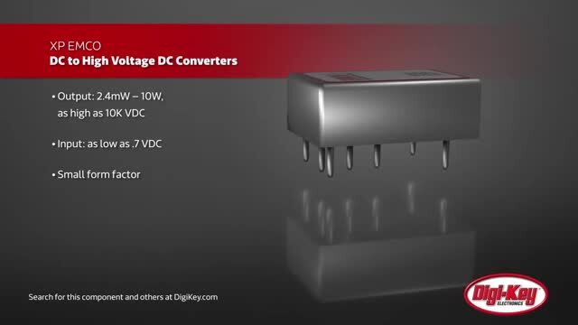
For these reasons, many engineers prefer to use a commercially available high voltage supply, such as the EMCO Series AG01P-5 from XP Power (Figure 2). This pc board mounted, small form factor unit has a profile of 0.128 inches (3.25 millimeters (mm)) and volume of under 0.100 cubic inches (1639 cubic mm). The supply operates from a DC source between 0.7 volts and 5 volts, yet delivers 100 volts at 10 mA. As an additional advantage, it is galvanically isolated to 500 volts, which is a requirement in many situations for proper system operation and user/equipment safety.

Figure 2: The tiny EMCO Series AG01P-5 DC/DC converter from XP Power takes a DC source from between 0.7 volts and 5 volts and produces 100 volts DC at 10 mA; it also includes 500 volts of isolation. (Image source: XP Power)
For applications which need higher voltage or current, XP Power and other vendors offer basic units which can supply hundreds and even thousands of volts at hundreds of mA. Some operate from a DC rail while many are AC line powered. By using a standard, off-the-shelf high voltage supply from a credible vendor, all of the technical performance and regulatory issues with the supply are effectively addressed. Therefore, the designers can instead focus on how to route the high voltage output from the supply to the circuitry it powers.
Of course, there are cases where an OEM-designed high voltage supply makes sense or is the only option. Examples include high volume applications where there may be cost benefits on the BOM; where a standard supply does not have the voltage/current pairing needed; systems which have unique space constraints or need a supply with unusual form factors; or where the OEM already has expertise in high voltage supply design and implementation. However, for most engineers, meeting the combination of technical requirements, selecting and sourcing unusual components, and managing regulatory issues makes the design of the high voltage supply a daunting task.
Providing the analog drive
Once the power rail sourcing is set, the next decision is how to provide the high voltage analog amplification needed by the load. Note that there are situations which need only a static DC voltage for bias and similar circuit requirements, but do not need a dynamic, controllable, amplified signal at high voltage. For these cases, just a supply (perhaps adjustable) is all that is needed.
The designer can choose three ways to implement a high voltage op amp function. The first approach is to use a standard low voltage op amp, but with booster transistors added on the output (Figure 3). This has the effect of converting the low voltage output swing to a wider, higher voltage range. Here, the Analog Devices LT1055 precision, high-speed op amp is used as the amplifier core, with the output boosted to a bipolar ±125 volt rail-to-rail span via three pairs of PNP/NPN transistors.

Figure 3: One approach to producing higher voltage op amp outputs is to add complementary booster transistors to the basic device, such as the LT1055, to take advantage of the input characteristics of the op amp. (Image source: Analog Devices)
This approach is viable and can do the job, but it requires a substantial number of additional active and passive discrete components. Further, the NPN/PNP transistor types selected must be matched with either similar or complementary specifications for gain, slew, and other parameters (depending on the specific parameter) to ensure symmetry in bipolar operation. Therefore, careful Spice or similar modeling of the design is necessary, including impact of component tolerance.
The second option is to use an op amp which is inherently designed for high voltage operation. While these are usually not monolithic parts due to semiconductor process limitations, they are packaged in a small module and are “dropped in” as a single component. These devices are often used in conjunction with a smaller, low voltage op amp which acts primarily as a signal buffer.
One example is the PB64 dual high voltage booster amplifier from Apex Microtechnology. Designed to provide voltage and current gain with a small-signal, general-purpose op amp (Figure 4), it is housed in a 12-pin electrically isolated SIP and measures 1.2 inches (31 mm) × 0.8 inches (20 mm) × 0.27 inches (7 mm), not including the through-hole pins. Typical applications include scientific instruments as well as testing of power semiconductors and LED/LCD arrays,

Figure 4: Although it is not a monolithic IC, a device such as the PB64 high voltage amplifier from Apex Technology is as easy to incorporate as a lower voltage device. (Image source: Apex Microtechnology)
The PB64’s maximum output voltage is ±75 volts, so it’s not as high as the discrete solution discussed earlier, but it has two relative benefits. It requires just a few non-critical passive components when used with a buffer, and it can deliver up to ±2 A, which is a significant amount of power (Figure 5).

Figure 5: In most applications, the high voltage PB64 amplifier is used with a standard op amp as an input buffer, to ensure a consistent input signal scenario and load. (Image source: Apex Microtechnology)
When examining the datasheets, look for critical static and dynamic performance characteristics such as safe operating area (SOA) and pulse response (Figure 6). Developing the equivalent data and specifications is time consuming and more difficult with the previous design approach.

Figure 6: Pulse response for the PB64 high voltage amplifier. (Image source: Apex Microtechnology)
The various higher voltage applications need different combinations of voltage and current, of course. For applications such as haptic piezoelectric transducers, the voltage needed may be higher than the Apex unit can provide, but the current demands are much lower. For these situations, an IC built on a high voltage process but with far less power dissipation capability may be a viable choice.
For example, due to its integrated boost converter, the Texas Instruments DRV8662 piezo haptic driver can swing up to ±200 volts into a 100 nanoFarad (nF) load (and will do higher capacitive loads but with reduced swing) from a power supply of just 3.0 to 5.5 volts (Figure 7).

Figure 7: Primarily targeting the niche application of driving piezo actuators for haptic designs, the DRV8662 IC from Texas Instruments delivers up to ±200 V to a capacitive load from a single-digit voltage source using its internal boost DC converter. (Image source: Texas Instruments)
This IC requires only a few external passive components and supports four GPIO controlled gains of 28.8 dB, 34.8 dB, 38.4 dB, and 40.7 dB. Despite its ±200 volt rating, it is housed in a tiny, 4 mm × 4 mm × 0.9 mm QFN package, making it well suited for portable applications where size is a factor and the available DC voltage rail is only a few volts. In a basic haptic application with a piezo transducer as an actuator, the drive signal could be set by a digital-to-analog converter (DAC) which is in turn controlled by a processor (Figure 8).

Figure 8: In addition to functioning as a basic analog high voltage driver, the DRV8662 includes four user-selected gain values to set the desired output range. (Image source: Texas Instruments)
Standards, regulatory mandates: a major issue
Unlike low voltage designs where there are minimal or no industry and government standards for user and system safety, the higher voltage world is tightly surrounded by them. Depending on the region of the world and end application, the specific standards will differ, but in general, designs under 50 to 60 volts have few or no restrictions (that’s one reason why the phone system settled on the still used 48 volt rail). Among the many standards setting organizations are UL, IRC, and the IPC.
However, as the voltages go higher, the increasingly strict requirements on physical arrangement of the design, as well as attention to electrical failure modes of the design and its mechanical structure become major issues. Most of the regulatory standards are focused on the voltage levels, not the current, since voltage is the primary source of risk to circuitry and to users. They closely align electrical (voltage) and mechanical design considerations.
These safety standards are focused on many issues, including:
- Will internal arrangement allow for arcing or flashover, and even possible combustion of materials?
- Will a mechanical or packaging failure (a stress crack, or crack after impact) expose the user to unsafe potentials?
- Will the higher internal voltages be accessible to a user?
Standards define minimum dimensions for “creepage and clearance” at various voltage levels (Figure 9). Creepage is the separation between two exposed points on the pc board as measured along the surface of the board, while clearance refers to the shortest distance between two conductive parts as measured through the air. As the voltages increase, the minimum distances also increase.

Figure 9: Creep and clearance are major considerations which affect layout and mechanical design in higher voltage circuits and systems; the basic minimum dimensions are just a starting point and are a function of voltage as well as other factors. (Image source: PCB Design Tech Guide)
However, there is much more to the creepage and clearance minimums than a simple table of “voltage versus distance.” The standards call out adjustments for circuit operating environment (dust, moisture, and other particulates), materials used, and other factors; it gets fairly complicated and confusing, so take the time to study the standards and any relevant guidelines.
A design which does not meet the relevant standards will not receive the critical certification. Of course, moving an exposed point or part even a millimeter on a pc board to meet mandates is often difficult and will likely have an unpleasant ripple effect on the design.
Therefore, it’s important to have a high voltage standards expert on staff or use a consultant who can evaluate and guide the project in its early stages, to avoid costly and time-consuming electrical and mechanical redesign and retesting.
Making the decision
Deciding which approach to use to develop higher voltages – booster transistors, hybrid module, or IC – is a function of many factors. First, can the selected approach support the top-tier parameters such as voltage, current, slew rate, and others? Second, what’s the skill of the team in designing and qualifying a high voltage analog amplifier design, solely from an electronic perspective? Third, can the design team identify and understand the relevant regulatory standards and their impact on the design?
The options and solutions discussed can provide various combinations of higher voltages and currents. However, in addition to the basic circuit designs, there are many external layout and placement issues that must be addressed at the early stages. These issues will also affect the high voltage amplifier approach which is ultimately selected.
Conclusion
While operating at lower voltages has many advantages, there is often a need to combine low and high voltage circuits. As shown, this can be done successfully and safely if the right approaches are taken with careful attention to product selection and implementation, as well as adherence to well-established standards.
Disclaimer: The opinions, beliefs, and viewpoints expressed by the various authors and/or forum participants on this website do not necessarily reflect the opinions, beliefs, and viewpoints of DigiKey or official policies of DigiKey.