How to Apply Third-Generation SiC MOSFETs to Power Designs for Higher Performance and Efficiency
Contributed By DigiKey's North American Editors
2022-11-02
There is a relentless drive for greater efficiency, smaller size, and enhanced performance across power applications such as industrial motor drivers, AC/DC and DC/DC inverters/converters, battery chargers, and energy storage systems. These aggressive performance requirements have surpassed the capabilities of silicon (Si) MOSFETs and ushered in newer transistor architectures based on silicon carbide (SiC).
While these newer devices offered significant benefits across key performance metrics, designers were wise to be wary of first-generation SiC devices due to various limitations and application uncertainties. Second-generation devices brought improved specifications along with a better understanding of device subtleties. As SiC MOSFET performance increased and time-to-market pressures intensified, designers used these newer devices to meet product objectives. More recently, third-generation devices are demonstrating the maturity of SiC-based power devices. These devices provide users with improvements across key parameters while also building on the design-in experience and related expertise of the previous generations.
This article compares Si to SiC, before discussing the development and migration to third-generation SiC MOSFETs. It then introduces real-world examples from Toshiba Semiconductor and Storage Corp. (Toshiba) to show how these devices can help designers achieve significant advances in power system design.
Silicon versus SiC
Over the past decades, the silicon-based MOSFET has transformed the design of power systems ranging from basic supplies and inverters to motor drives. Along with the insulated gate bipolar transistor (IGBT)—a functionally similar semiconductor but with very different construction and attributes—the switching optimized Si MOSFET has enabled a transition from traditional, inefficient power conversion and management based on linear topologies, to a much more efficient and compact approach using switched control.
Most of these designs use a form of pulse-width modulation (PWM) to deliver and maintain the desired voltage, current, or power value in a closed-loop feedback arrangement. As the use of silicon MOSFETs grew, the demands placed on them also increased. In addition, new efficiency goals (many based on regulatory mandates), the markets for electric vehicles and smarter motor control, power conversion for renewable energy and associated energy storage systems, have pushed these MOSFETs to do more and better.
As a result, a considerable amount of R&D effort has improved the performance of silicon-based MOSFETs, but researchers realized that this effort was reaching the point of diminishing returns. Fortunately, they had an alternative, in theory, based on power-switching devices that used SiC as the substrate rather than silicon alone.
Why use SiC?
For various deep-physics reasons, SiC has three major electrical characteristics that differ significantly from silicon alone, and each brings operational advantages; there are also other, more subtle differences (Figure 1).
") Figure 1: Approximate comparison between key material properties of SiC versus Si and gallium nitride (GaN) solid materials. (Image source: Researchgate)
Figure 1: Approximate comparison between key material properties of SiC versus Si and gallium nitride (GaN) solid materials. (Image source: Researchgate)
The three main characteristics are:
- Higher critical breakdown electric-field voltage of about 2.8 megavolts/centimeter (MV/cm) versus 0.3 MV/cm, so operation at a given voltage rating is possible with a much thinner layer, greatly reducing drain-source “on” resistance (RDS(on)).
- Higher thermal conductivity, enabling higher current density in a cross-sectional area.
- Wider bandgap (the energy difference in electron volts between the top of the valence band and the bottom of the conduction band in semiconductors and insulators), resulting in lower leakage current at high temperatures. For this reason, SiC diodes and field effect transistors (FETs) are often referred to as wide bandgap (WBG) devices.
As a result, SiC-based devices can block voltages up to ten times higher than silicon-only structures, they can switch about ten times faster, and they have an RDS(on) of half or less at 25°C while utilizing the same die area (all approximate figures, of course). Also, the turn-off switching-related loss of SiC devices is less because there is no detrimental tail current. At the same time, their ability to operate at much higher temperatures of roughly 200°C, versus 125°C, eases thermal design and management issues.
Due to their performance attributes and advances, SiC devices have now taken a prominent place in the power vs. speed application matrix, joining IGBTs, silicon MOSFETs, and GaN devices (Figure 2).
 Figure 2: The performance attributes of SiC MOSFETs make them suitable for a broad range of applications encompassing a span of power and frequency ratings. (Image source: Toshiba)
The path from the underlying SiC materials science and device physics to commercial SiC MOSFETs was not quick or easy (Figure 3). After extensive research and production efforts, the first SiC-based devices—Schottky diodes—were introduced in 2001. In the two decades after that, the industry developed and released production volumes of first, second, and third-generation SiC MOSFETs. Each generation offers targeted improvements in specific parameters, along with somewhat different tradeoffs.
") Figure 3: The story of commercial SiC-based devices begins with the first commercial SiC Schottky diodes, which appeared in 2001. (Image source: IEEE Transactions on Industrial Electronics, 2017)
Figure 3: The story of commercial SiC-based devices begins with the first commercial SiC Schottky diodes, which appeared in 2001. (Image source: IEEE Transactions on Industrial Electronics, 2017)
Note that it’s important to be clear about terminology: just like their silicon-only predecessors, SiC-based FETs are MOSFETs. In the broad sense, their internal physical structures are similar, and both are three-terminal devices with source, drain, and gate connections. The difference is as their names indicate: SiC-based FETS use SiC as their base material rather than silicon alone.
Begin with first and second generations
There are many parameters that characterize the performance of a switching device. Among the many static parameters are the maximum operating voltage and the maximum current rating, along with two static Figures of Merit (FoMs): the RDS(on) and the maximum operating temperature, which are related to the power handling capability for a given die size and package.
As switching devices, dynamic parameters are also critical as they are needed to assess switching losses. The most-cited dynamic FoM is the product of the RDS(on) and the gate charge, RDS(on) × Qg, while an increasingly important one is the reverse recovery charge, Qrr. The sizing and capabilities of the gate driver needed to properly source and sink current to the switching device—and do so without overshoot, ringing, or other distortions—is primarily determined by these FoMs.
The use and market growth of first-generation SiC devices had been held back by reliability issues. One of these involves PN diodes, which are positioned between a power MOSFET’s power source and drain. Voltage applied to the PN diode energizes it, resulting in a change of on-resistance that degrades device reliability.
Toshiba’s second-generation modified the basic SiC device structure by using a Schottky barrier diode (SBD) embedded in the MOSFET to largely solve this problem (Figure 4). This improved reliability by more than an order of magnitude. The new structure prevented energizing of the PN diode by positioning the SBD in parallel with the PN diode inside the cell. Current flows through the embedded SBD because its on-state voltage is lower than that of the PN diode, thus suppressing some changes in on-resistance and degradation of the MOSFET’s reliability.
 (left), the one with it (right)") Figure 4: Unlike the typical SiC MOSFET without an internal Schottky barrier diode (SBD) (left), the one with it (right) can minimize the energization of the parasitic PN diode. (Image source: Toshiba)
Figure 4: Unlike the typical SiC MOSFET without an internal Schottky barrier diode (SBD) (left), the one with it (right) can minimize the energization of the parasitic PN diode. (Image source: Toshiba)
MOSFETs with embedded SBDs were already in practical use, but only in high voltage products—such as 3.3 kilovolt (kV) devices—as the embedded SBD caused on-resistance to eventually rise to a level that only high-voltage products can tolerate. Toshiba adjusted various device parameters and found that the ratio of the SBD area in a MOSFET is the key to suppressing the increased on-resistance. By optimizing the SBD ratio, Toshiba devised a 1.2 kV class SiC MOSFET with noted improvement in reliability.
However, as with many enhancements, there were tradeoffs. While the new device structure significantly improved reliability, it also had a detrimental effect on two FoMs. It increased nominal RDS(on) as well as RDS(on) × Qg, reducing the performance of the MOSFET. To compensate for and reduce the on-resistance, second-generation SiC MOSFETs had increased die area, but this increased cost.
Third generation shows true maturity
Acknowledging this concern, Toshiba developed a third-generation of SiC MOSFET devices, called the TWXXXN65C/TWXXXN120C family. These devices optimized the structure of the current-spreading layer to reduce the cell size and also deliver a higher voltage rating, faster switching, and lower on-resistance.
On-resistance is lowered in part by reducing the spread resistance (Rspread). The SBD current is increased by injecting nitrogen into the bottom of the wide P-type diffusion region (P-well) of the SiC MOSFET. Toshiba also reduced the JFET region and injected nitrogen to reduce feedback capacitance and JFET resistance. As a result, feedback capacitance was reduced without increasing on-resistance. Stable operation without fluctuation of on-resistance was also obtained by optimized positioning of the SBD.
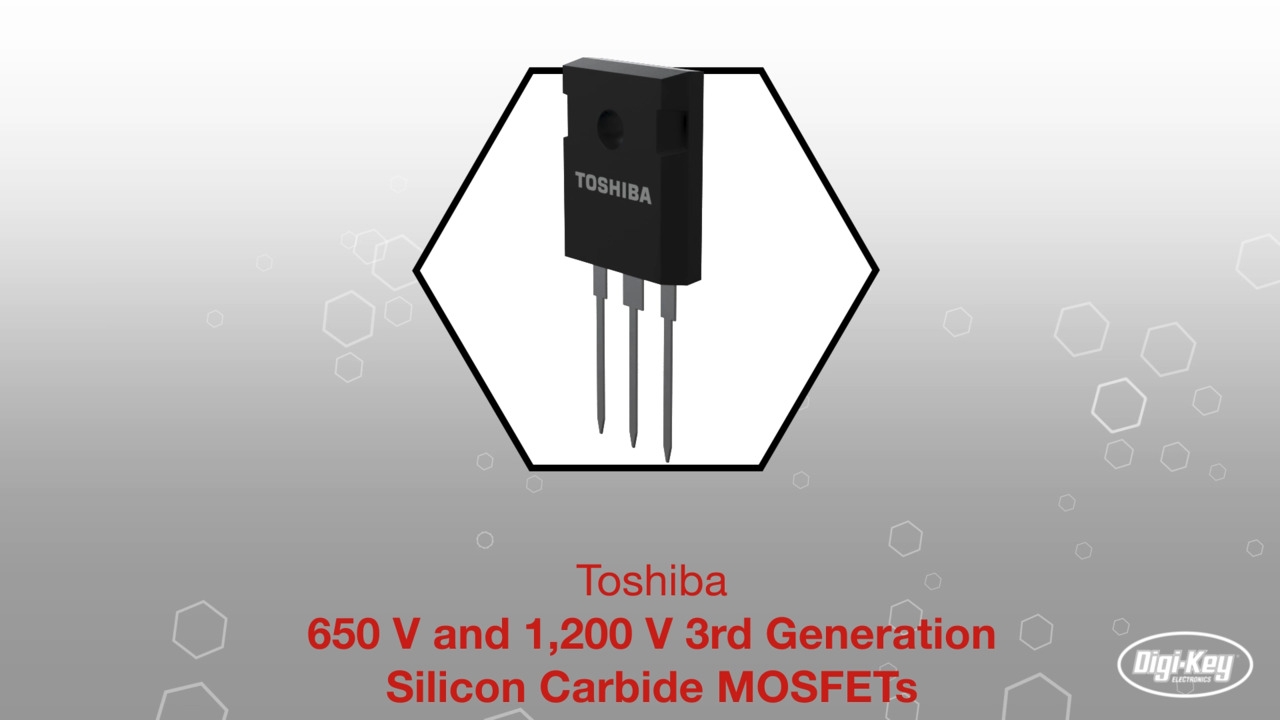
At present, the family consists of 650-volt and 1,200-volt SiC MOSFETs designed for high-power industrial applications such as 400-volt and 800-volt AC/DC power supplies, photovoltaic (PV) inverters, and bi-directional DC/DC converters for uninterruptible power supplies (UPSs). Both the 650-volt and 1,200-volt SiC MOSFETs are offered in the industry standard three-lead TO-247 package (Figure 5).
 Figure 5: Housed in a standard T0-247 package, the Toshiba 650 volt and 1200 volt third-generation SiC MOSFETs are well-suited to a wide range of power conversion, control, and management applications. (Image source: Toshiba)
In these third-generation SiC MOSFETs, the RDS(on) × Qg FoM is reduced by 80% compared to Toshiba’s second-generation devices—a significant drop—while switching loss is reduced by about 20%. The built-in Schottky barrier diode technology also offers ultra-low forward voltage (VF).
There are other design-in subtleties associated with MOSFETs. Take VGSS, for example. VGSS is the maximum voltage that can be applied between the gate and source while the drain and source are short-circuited. For third-generation SiC devices, the VGSS range is 10 to 25 volts, with 18 volts as the recommended value. The wide VGSS ratings help make design easier while improving design reliability.
Further, the low resistance and a higher gate threshold voltage (VGS(th))—the voltage at which the MOSFET channel begins to conduct—helps prevent malfunctions, such as accidental turn-on due to spikes, glitches, and overshoots. This voltage ranges from 3.0 to 5.0 volts, helping to ensure predictable switching performance with minimal drift while permitting a simple gate-driver design.
A closer look at 650-volt and 1200-volt third-gen SiC MOSFETs
A look at two devices at opposite ends of the family spectrum, the 650-volt and 1200-volt devices shows the span of their capabilities. The physical package, pinout, and schematic symbol for all of them is the same (Figure 6), but the specifics differ.
 Figure 6: All members of Toshiba’s third-generation SiC MOSFET family have the same physical arrangement and schematic symbol; note the integral Schottky barrier diode in the symbol. (Image source: Toshiba)
One 650-volt device is the TW015N65C, an N-channel device rated at 100 amperes (A) and 342 watts. Its typical specification values are an input capacitance (CISS) of 4,850 picofarads (pF), a low gate-input charge (Qg) of 128 nanocoulombs (nC), and a nominal RDS(on) of just 15 milliohms (mΩ).
Along with tables of minimum, typical, and maximum figures for static and dynamic parameters, the datasheet has graphs that show the performance of critical parameters versus factors such as temperature, drain current, and gate-source voltage (VGS). For example, the value of RDS(on) versus temperature, drain current (ID), and gate-source voltage VGS is shown in Figure 7.
") Figure 7: Shown are graphs that characterize on-resistance for the TWO15N65C from different perspectives, including drain current, ambient temperature, and VGS. (Image source: Toshiba)
Figure 7: Shown are graphs that characterize on-resistance for the TWO15N65C from different perspectives, including drain current, ambient temperature, and VGS. (Image source: Toshiba)
The same set of specifications and graphs are shown in Figure 8 for the 1200 volt devices, such as the TW140N120C, a 20 A, 107-watt, N-channel device. This SiC MOSFET features a low CISS of 6000 pF, a gate-input charge (Qg) of 158 nanocoulombs (nC), and an RDS(on) of 140 mΩ.
") Figure 8: On-resistance characterization graphs for the TW140N120C. (Image source: Toshiba)
Figure 8: On-resistance characterization graphs for the TW140N120C. (Image source: Toshiba)
The ten available third-generation Toshiba SiC MOSFETs comprise five 650-volt devices along with five 1200-volt devices. At 25°C, they have the following on-resistance, current, and power ratings:
650-volt:
- 15 mΩ, 100 A, 342 watts (the TWO15N65C)
- 27 mΩ, 58 A, 156 watts
- 48 mΩ, 40 A, 132 watts
- 83 mΩ, 30 A, 111 watts
- 107 mΩ, 20 A, 70 watts
1200-volt:
- 15 mΩ, 100 A, 431 watts
- 30 mΩ, 60 A, 249 watts
- 45 mΩ, 40 A, 182 watts
- 60 mΩ, 36 A, 170 watts
- 140 mΩ, 20 A, 107 watts (the TW140N120C)
Conclusion
Silicon carbide MOSFETs offer a significant improvement in critical switching parameters, relative to silicon-only devices. Compared to previous generations, third-generation SiC components offer improved specifications and FoMs, enhanced reliability, better characterization of gate-driver requirements, and greater insight into inevitable design-in subtleties. Using these SiC MOSFETs, designers of power systems have an additional core resource they can use to achieve higher efficiency, smaller size, and improved overall performance.
Disclaimer: The opinions, beliefs, and viewpoints expressed by the various authors and/or forum participants on this website do not necessarily reflect the opinions, beliefs, and viewpoints of DigiKey or official policies of DigiKey.