Get Embedded Microprocessor/FPGA Combo Designs Up and Running Fast with SoMs
Contributed By DigiKey's North American Editors
2018-07-25
Many embedded designs can make use of single board computers (SBCs) and systems on modules (SoMs) based on microprocessors and microcontrollers (for example, see “Build a Low-Cost Industrial Controller with the Raspberry Pi 3”). However, many more embedded applications cannot tolerate the latencies associated with software-dependent response times.
These applications need the extra performance only available with custom hardware, and the fastest way to develop custom hardware is using an FPGA.
This article will discuss the advantages of using SoMs for developing embedded systems that need the extra processing power provided by FPGAs. It will also introduce a variety of FPGA SoMs and will discuss their use in the development of embedded designs.
The role of an FPGA system on module
A SoM helps designers develop embedded systems with custom interfaces in a form factor without the effort of developing a core processing system from the ground up. Designers can plug a predesigned and tested SoM into either a predesigned or a custom carrier card to create an embedded design that functions identically to one that is fully custom engineered. However, the hardware development will require much less time.
There are a number of benefits to using a SoM versus developing hardware from the ground, up. These include:
- Cost savings (when considering the total NRE costs incurred in developing and debugging a board based on an SoC)
- Reduced design risk
- Multiple SoC choices (due to the SoM’s pluggability)
- Small footprint
- Parallel hardware and software development
SoMs now occupy the niche once occupied by microprocessors and microcontrollers when through-hole and socketable parts dominated. Pin compatibility permitted a designer to select from a range of compatible processors with the right processor clock rate and just the right amount of memory on chip. However, higher pin counts and surface mount packaging have obsoleted that design approach, and opened a door for the creation of SoMs with form factors and footprints that serve the same purpose as the earlier pin-compatible microcontroller families.
By using a SoM for the project’s computing platform, design engineers can focus their efforts and resources on developing the final application instead of becoming mired in the details of designing a computing platform. For example, at clock rates of several hundred megahertz, board layout for SDRAMs coupled to the application processor becomes increasingly difficult due to differential trace delays, noise, crosstalk, and a host of other challenges. Meanwhile, SoM vendors have already met these challenges and shortened the time to market by getting much of the design done before the project has started.
Choosing a SoM family for an embedded development project requires careful analysis of factors including anticipated embedded resource requirements, the need for design scalability and future proofing, and ease of use. It helps to pick a SoM form factor and footprint that provides ample selection alternatives for the known challenges and for unanticipated future challenges. Choosing a multi-member SoM family with a compatible form factor and connector footprint expands the design team’s choices and provides for additional future proofing.
A new type of SoM based on SOCs with processors and FPGAs
SoMs often incorporate SoCs with multiple application processors, but a new class of embedded processor SoCs that incorporate an FPGA, such as the Xilinx All Programmable Zynq®-7000 SoC, is also appropriate for SoM design. Xilinx Zynq-7000 SoCs integrate the software programmability of an Arm® Cortex®-A9 application processor with the hardware programmability of an FPGA. The Zynq SoC’s built-in Arm microprocessors, coupled with hardened peripherals and an SDRAM memory controller called the Zynq SoC’s “processing system" or “PS,” execute all of the software-based tasks normally handled by an embedded microprocessor or microcontroller, while the integrated FPGA (called the Zynq SoC’s “PL” for “programmable logic”) provides hardware I/O response times and hardware acceleration for embedded tasks that require faster execution.
Xilinx Zynq SoCs are available with a variety of processor configurations and speeds, with even more variety in terms of the amount of FPGA fabric available on the chip. Choosing a SoM family based on a hybrid processor/FPGA SoC like the Xilinx Zynq-7000 family expands choices and improves future proofing just that much more.
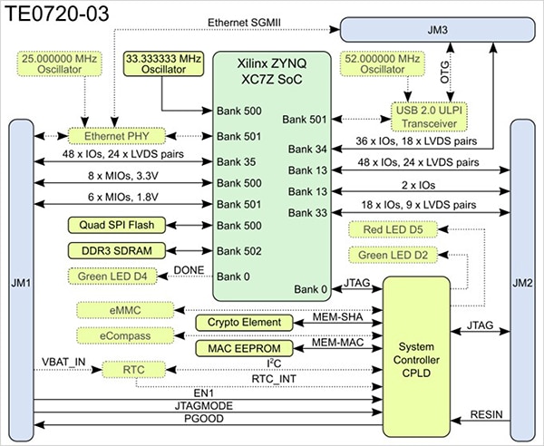
One such SoM family is the TE0720 Series (Figure 1) and companion SoM carrier board, the TE0703 from Trenz Electronic. All of the SoMs are based on a common form factor measuring 4 x 5 centimeters (cm). The modules in the Trenz Electronic TE0720 series incorporate one of two members from the Xilinx Zynq-7000 SoC family:
- The TE0720-03-2IF based on the Xilinx Zynq Z-7020 SoC
- The TE0720-03-1QF based on the Xilinx Zynq Z-7020 SoC
- The TE0720-03-1CR based on the Xilinx Zynq Z-7020 SoC
- The TE0720-03-1CFA based on the Xilinx Zynq Z-7020 SoC
- The TE0720-03-2IFC3 based on the Xilinx Zynq Z-7020 SoC
- The TE0720-03-L1IF based on the Xilinx Zynq Z-7020 SoC
- The TE0720-03-14S-1C based on the Xilinx Zynq Z-7014S SoC
All of these SoMs have a common connector footprint that incorporates three Samtec LSHM hermaphroditic connectors carrying several hundred I/O pins, plus power and ground pins between the SoM and the carrier board.

Figure 1: The Trenz Electronic TE0720 SoM incorporates either the Xilinx Zynq Z-7020 or Z-7014S SoC along with 1 Gbyte of SDRAM and additional nonvolatile memories. (Image source: Trenz Electronic)
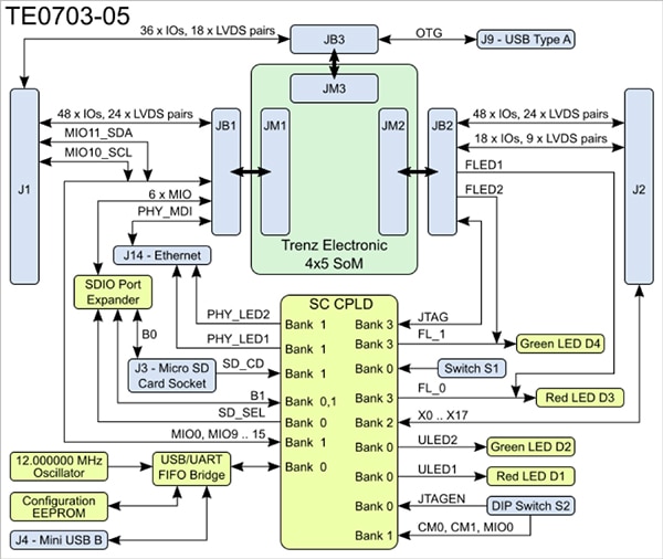
Perhaps the best way to appreciate the flexibility of the SoM design approach is to look at the TE0703 carrier board for the TE0720 SoM series and then work back into the SoM through the I/O pins to look at the SoM’s resources (Figure 2).

Figure 2: The Trenz TE0703 carrier board breaks out the many I/O pins from the associated 4 x 5 cm SoM board to the rest of the embedded system. (Image source: Trenz Electronic)
The block diagram of the TE0703 shows the numerous significant I/O capabilities broken out from the SoM board including:
- 1 Gbit/s Ethernet
- USB and Mini USB
- Micro SD card
- Hundreds of I/O pins (configurable as individual digital I/O pins or as low-voltage differential signaling pairs (LVDS))
SoMs and SBCs each have their place
Processing speed, response time, and I/O capabilities are distinguishing characteristics of SoMs. However, SBCs such as the Arduino Uno and the Raspberry Pi family, are also frequently incorporated into embedded systems as they also come with a broad base of support. As a result, Trenz Electronic also offers versions of the Arduino and Raspberry Pi boards, the TE0723-03M ArduZynq and the TE0726-03M ZynqBerry, that are based on a Xilinx Zynq-7000 SoC. These SBCs provide a bridge to many existing plugin cards such as Arduino shields and Raspberry hats and bonnets.
There’s a significant difference in the amount of FPGA capability between the Zynq Z-7010 SoCs incorporated into the TE0723-03M ArduZynq and the TE0726-03M ZynqBerry SBCs, compared to the capabilities built into the TE0720 series Trenz Electronic SoMs, which incorporate the Zynq Z-7014S, Zynq Z-7020 SoC devices. Although all of the Zynq-7000 SoCs incorporate a dual-core Arm Cortex-A9 processor, the devices differ in the amount of FPGA on the device, as shown in Table 1:
|
Table 1: The Xilinx Zynq-7000 SoCs used in Trenz Electronic’s SOMs (the Z-7014S and Z-7020) have many more FPGA resources than the Zynq Z-7010 used in the Trenz Electronic ArduZynq and ZynqBerry SBCs. (Data source: DigiKey)
In addition, the TE0723-03M ArduZynq and the TE0726-03M ZynqBerry SBCs have 512 Mbytes of SDRAM on board while the TE0720 SoMs have 1 Gbyte.
Trenz Electronic supplies multiple carrier boards for its SoMs, including the TE0703-05, TE0706-02, TE0701-06, and TEB0745-02. These boards provide a wide range of standardized I/O capabilities. One of these carrier cards might be appropriate for a certain embedded application, but it’s also possible to partition the design of the embedded system into a custom designed carrier board that accepts the range of SoMs within a family to meet different processing needs. This flexibility underscores the utility of a design approach based on using a SoM family as the foundation of an embedded design. The SoM’s consistent and standardized connector footprint permits easy interchange of one SoM for another to accommodate changes in the system specification.
Conclusion
SoMs can greatly reduce the time required to prototype embedded systems and reduce project risk. Once a SoM form factor and connector footprint are adopted, SoMs with increased amounts of FPGA resources can be plugged in to meet expanding needs. Additionally, a variety of compatible SoMs based on Xilinx Zynq-7000 SoCs, which combine the processing power of a dual-core Arm Cortex-A9 processor with FPGA resources, can also help accelerate development in embedded designs.
This SoM to embedded design not only shortens the amount of time needed to develop the hardware portion, it also permits software development to start earlier in the project, and thus reduces design risk. It also provides good flexibility should the project’s scope and requirements happen to grow.

Disclaimer: The opinions, beliefs, and viewpoints expressed by the various authors and/or forum participants on this website do not necessarily reflect the opinions, beliefs, and viewpoints of DigiKey or official policies of DigiKey.


