Choosing and Using the Right Flash Memory Technology for IoT Program Memory Applications
Contributed By DigiKey's North American Editors
2018-05-23
As IoT nodes have become more powerful, the processing requirements can increase to a level that requires a full embedded operating system (OS) such as Linux to properly manage the complexity of all the running tasks. While it’s convenient to store this code on a flash microSDHC card, most flash microSDHC cards are designed only for data storage and not OS storage, though vendors have come up with some innovative solutions.
This article describes the role of an embedded OS and why it’s often wise to put both the OS and application code on a microSDHC flash card in an IoT node. It then explains the mode of deterioration of flash cards and how OSes can be particularly affected by this deterioration phenomenon. It then shows how designers can use new flash memory implementations to overcome this deterioration for efficient as well as reliable IoT node implementations.
Why use an embedded OS
For some IoT applications, the more pre-processing that can be performed at the remote IoT node, the less data the IoT node needs to transmit back to the central hub, freeing up network bandwidth. A pre-tested embedded OS can support complex pre-processing by handling many individual tasks efficiently, and can multitask in a predictable (deterministic) manner. This will, of course, place extra demands on the microcontroller, requiring a faster clock speed and more importantly, more program memory.
A commercial or open-source off-the-shelf embedded OS can also have the advantage of solid, pre-tested code that rarely needs updating. For example, available embedded Linux OSes might only be updated quarterly, or only for emergency security patches. An embedded OS and the required application code can require 8 Gbytes or more, and since the OS is rarely updated it can be more convenient to store the OS on a microSDHC flash memory card that is manually (physically) updated by a technician. This also scales for future memory expansion, as an existing 4 Gbyte flash card can easily be replaced with an 8 Gbyte or larger card if needed the next time the technician visits (Figure 1).
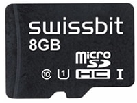
Figure 1: A Swissbit Class 10 microSDHC S-140u memory card which supports speeds of up to 104 MBytes/s, fast enough for high-speed program memory access. (Image source: Swissbit)
Storing gigabytes of an embedded OS on a microSDHC NAND flash card that is updated physically has several advantages over flash memory updated over a wireless network. In a wireless network, depending on the arbitration scheme used, updating a 4 Gbyte or more embedded OS might steal wireless bandwidth from operational communications. Updating over a network also requires a microSDHC card that is twice the normal size, as it needs enough storage to both run the OS as well as accommodate the incoming update.
Updating flash code over wireless also reduces battery life because of the radio activity, as well as the higher flash write voltages and power requirements.
An embedded OS executing out of flash memory also places different demands on the flash memory cells compared to data storage. Most commercial flash microSDHC cards are designed by the manufacturer only for data storage. The most common commercial use is multimedia storage for mobile devices. While multiple bit errors in a video, image, or audio file can go unnoticed to the end user, a single bit error in a critical embedded OS file can result in total system failure.
Flash memory does not have an unlimited lifespan. Each write operation to a flash memory array decreases the lifespan of the array. Each semiconductor flash memory specification lists a limited number of erase/write cycles. As the flash cell approaches that spec’ed limit, the cell becomes more and more likely to wear out and not accept a new programming state.
One common approach to prevent the deterioration of the flash array due to write operations is called wear leveling. Instead of writing to the same flash location, writes are evenly distributed across the entire flash semiconductor memory array, ensuring an even distribution of writes across the flash memory matrix. With wear leveling, as the microcontroller writes to a single location in physical memory, the flash controller can map that same location to different locations in the flash memory array.
How read disturb errors occur
OS files are accessed much more frequently than data files, so they can be unforgiving when it comes to file bit errors. In some cases, core OS files might be read constantly, and this can introduce bit errors in the flash array.
Flash memory is arranged in blocks, and each block contains a number of pages. Blocks are the smallest parts of memory that can be erased, while pages are the smallest parts of memory that can be read or programmed. A common size for a flash block is 256 KBytes, which may contain 64 pages of 4 Kbytes each. Every page also includes an extra 64 bytes used for error correcting code (ECC), erase counts, and logical to physical translation information.
During a flash read operation of a page of data, a small read voltage is applied to the entire block the page belongs to, even if only one byte in the page needs to be read. Because of the flash process cell technology, this also induces a smaller voltage into the surrounding pages in the block. This can inject electrons into the cell insulation layers, similar to programming the cell, which is why it is referred to as “soft programming”. Repeatedly applying the small read voltage to the same block can eventually disturb the programming of the flash pages not being read. Over time, this can result in changing the state of the adjacent cells to a different value.
While most NAND flash microSDHC cards have some form of error correction to correct cell errors, the number of errors caused by soft programming can be so numerous that it can reach a critical level that cannot be corrected, resulting in the microcontroller reading a different value from the bit location, resulting in a file corruption error. These bit errors are referred to as read disturb errors.
A NAND flash microSDHC card used for data storage rarely sees read disturb errors. Because of the write operations performed on the flash array, after a wear leveling operation, the flash locations are reprogramed, eliminating any soft programming effects. However, a flash array used for an embedded OS is so rarely programmed that a read disturb error can become a reality.
Single-level cell (SLC) flash cards are rated at one million reads, and multi-level cell (MLC) flash cards are rated at 100,000 reads before a read disturb error would occur. For data flash, a read disturb error is considered so rare that these figures are often not specified on the data sheets.
Use RDM to prevent read disturb errors
To prevent read disturb errors, Swissbit developed a feature called Read Disturb Management (RDM). In Swissbit’s RDM, the flash card controller keeps track of the number of read operations for each individual flash block. When a block reaches an internally defined number of read operations, the controller moves the data to a new block, similar to wear leveling used for write operations. If necessary, during the write operation to a new block, the SD controller’s error correcting code (ECC) corrects any corrupted data.
RDM has been implemented in Swissbit’s SFSD8192N1BM1MT-I-QG-221-STD 8 Gbyte S-450u UHS-I Class 10 microSDHC flash card. Designed specifically for industrial applications using embedded OSes, the S-450u has enough room for an embedded Linux OS and application code for many complex IoT nodes. In SDR104 mode, the S-104u can support up to 104 Mbytes/s data access.
Using a microSDHC card for program memory execution
As explained earlier, microSDHC cards are usually only used for data memory, so the peripherals on most Harvard architecture microcontrollers only support accessing microSDHC cards as data memory. This limits available options.
Existing solutions read the microSDHC card and load the program memory into RAM, and then execute out of RAM. Not only does the RAM chip add extra cost to the board, but program expansion is limited to the amount of on-board RAM available on the pc board.
MicroSDHC cards are capable of interfacing in SD mode or SPI mode.
To interface the microcontroller to the S-450u microSDHC card as program memory, the microcontroller selected would need to support one of the two microSDHC bus protocols:
- An SDHC card SD Mode controller peripheral mapped to program memory (Figure 2). This can be an external peripheral, or an internal microcontroller peripheral. The interface consists of six signals: four bits of data (DAT[0-3]), a clock (CLK), and a bi-directional Command/Response signal (CMD). Data is transferred four bits at a time and provides the fastest program execution speed. The host controller or microcontroller provides the clock to the microSDHC card.
- A configurable SPI interface with eXecute In Place (XIP) support. This can execute code from the card by accessing the microSDHC card in SPI mode, providing a fast transfer of data, but not as fast as an SDHC card mode. XIP memory maps the card’s memory into the microcontroller’s program memory space, making access to the microSDHC card transparent to the host firmware.
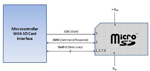
Figure 2: Interfacing to a microSDHC card using SD Mode uses a simple six signal interface to provide the fastest memory access. (Image source: DigiKey)
A microSDHC card powers up in SD card mode. To select single-bit SPI mode, on the first six clocks after power-up the DAT3 signal must be pulled up to VDD, while at the same time a RESET command (000000b) is sent to the card by pulling CMD down to VSS. After this the card stays in SPI mode until it is powered off.
The MAX32652 Arm® Cortex®-M4F microcontroller from Maxim Integrated is a low-power microcontroller designed for IoT nodes. It features an on-chip QSPI XIP interface that if properly configured is capable of executing code out of a microSDHC card.
The MAX32652 also features a full SDHC interface primarily for data memory storage.
It’s important to note that these interfaces to the microcontroller must be program memory interfaces. Regardless of the bus protocol or interface used, the microcontroller would need to contain some on-chip flash boot code to initialize the interface to the microSDHC card.
Socketed safety
The socket for an industrial application microSDHC card is often overlooked. For rugged applications, tin or similar contact materials can tarnish or lose their tensile strength over time. Gold contacts, while costing a few pennies more, are worth the cost by providing a solid contact connection that keeps its tensile strength over time.
The 10101704J6#2A Universal Flash Storage (UFS) and microSDHC connector/socket from Amphenol ICC provides a solid connection for any microSDHC-compatible card (Figure 3). This socket features anti-stubbing contacts which prevent memory cards getting stuck during insertions and withdrawals.
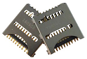
Figure 3: The 10101704J6#2A UFS and microSDHC card connector/socket supports both existing microSDHC and the next-generation UFS cards with data transfer speeds of up to 6 Gbytes/s. (Image source: Amphenol)
This Amphenol socket also supports future expansion by having compatibility with the new Universal Flash Storage (UFS) format, which has a similar form factor as microSDHC but has a different contact footprint (Figure 4). The UFS card supports twice the speed of microSDHC with differential bi-directional data transfer.
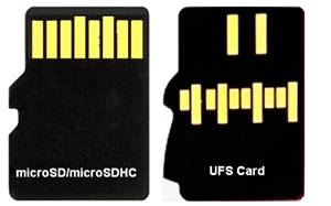
Figure 4: A microSDHC card on the left, and the new UFS card on the right. The UFS card supports twice the speed of microSDHC with differential bi-directional data transfer. (Image source: DigiKey)
Some networked IoT nodes might be in remote locations where Wi-Fi is unavailable or impractical. For these situations, networking could be performed over a wireless cellular data connection. This requires the use of a subscriber SIM card, which also needs to be socketed.
A simple way to save board space would be to use a combination microSDHC and SIM card socket like the 1041681620 dual SIM card and microSDHC card socket from Molex (Figure 5). This socket also features gold contacts for a solid connection in harsh environments and anti-stubbing contacts.
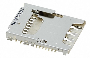
Figure 5: The 1041681620 combination SIM card and microSDHC card socket significantly reduces board space and provides anti-stubbing contacts to prevent insertion and withdrawal errors. (Image source: Molex)
Conclusion
While flash microSDHC cards have been used for data storage, they are now improving to support the unique needs of executing program memory in place for embedded OSes. Part of that evolution includes the development of faster flash memories that can support constant read requests. Also, microcontrollers are evolving to support new memory interfaces that can reliably execute code from an external microSDHC card, while reducing or eliminating flash errors.

Disclaimer: The opinions, beliefs, and viewpoints expressed by the various authors and/or forum participants on this website do not necessarily reflect the opinions, beliefs, and viewpoints of DigiKey or official policies of DigiKey.


